

Custom Power Bank |6| Advanced Power Bank (APB) Boards Acceptance
Intro
This series of notes describes developing process of custom power bank.
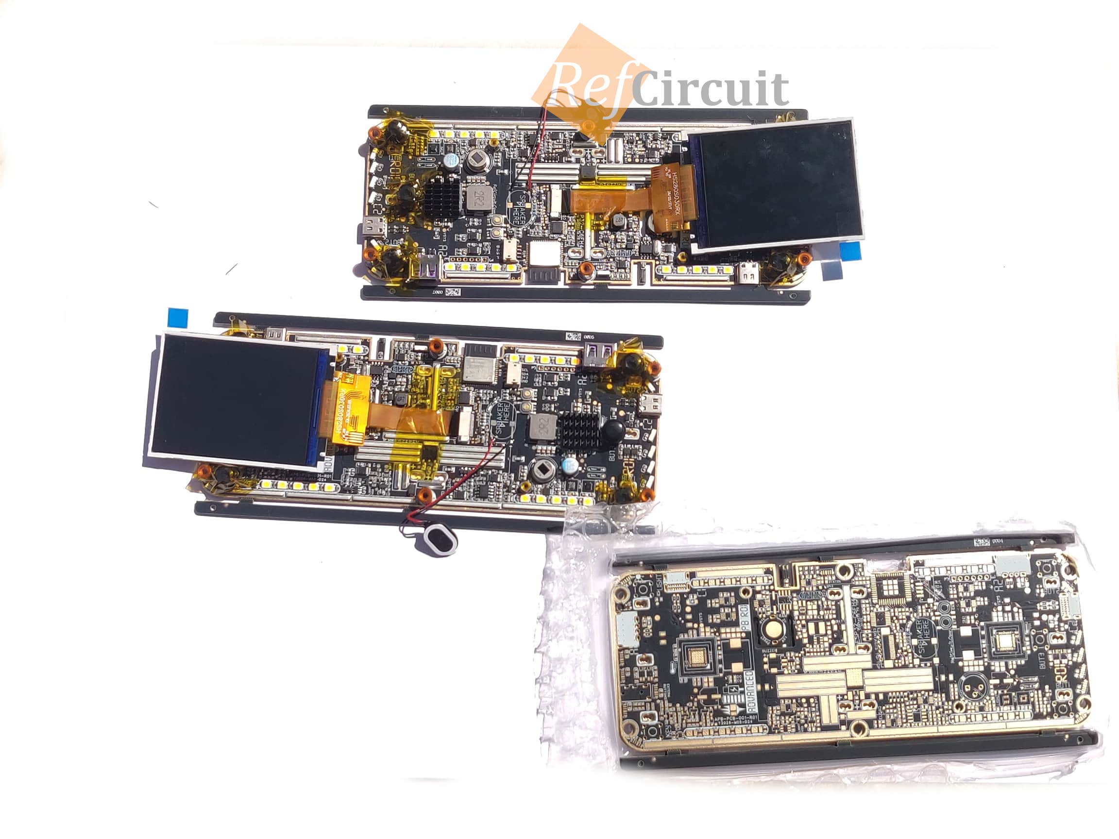
Purpose: acceptance and checking assembled boards (PCBA) of custom power bank.
Specs
- Size: 180x68mm
- Thickness: 1.6mm
- PCB Color: Black
- Silkscreen: White
- Stackup: JLC04161H-7628
- Material Type: TG135
- Outer Copper Weight: 1 oz
- Inner Copper Weight: 0.5 oz
- Via Covering: Plugged
- Surface Finish: ENIG Gold Thickness: 1U"
- Edge Plating: Yes
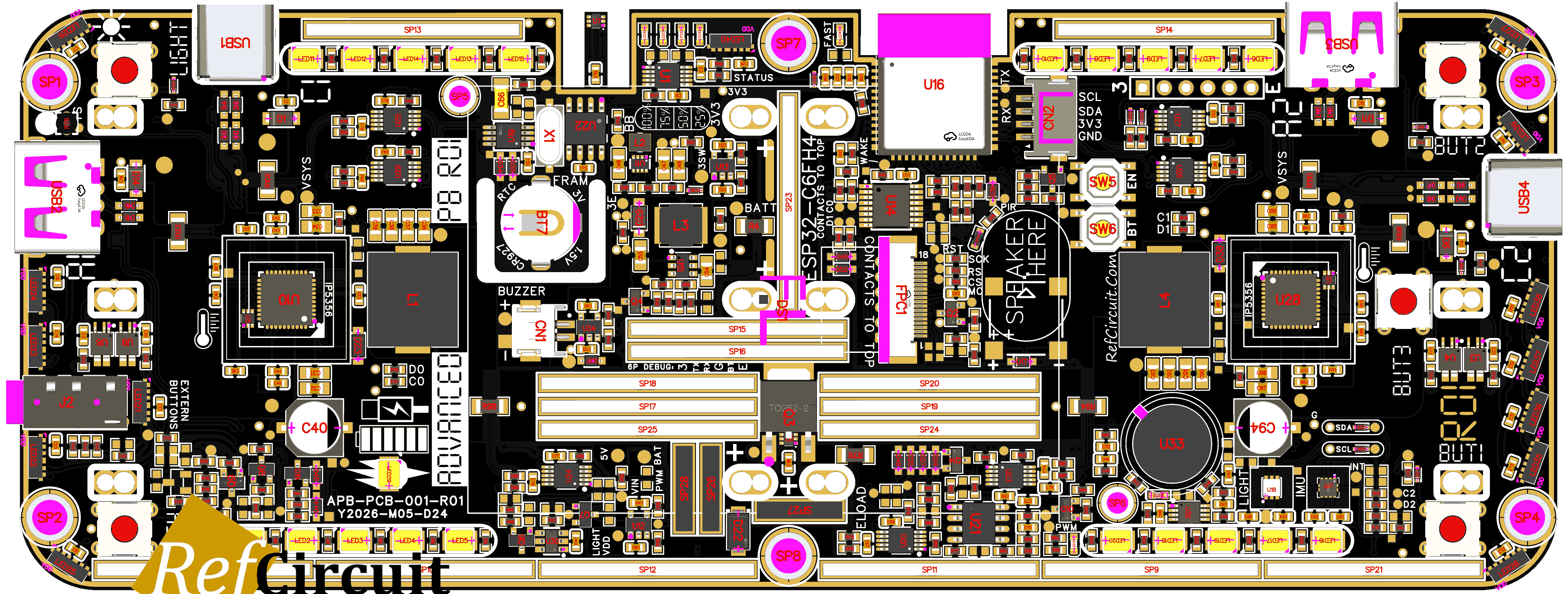
Board
 |
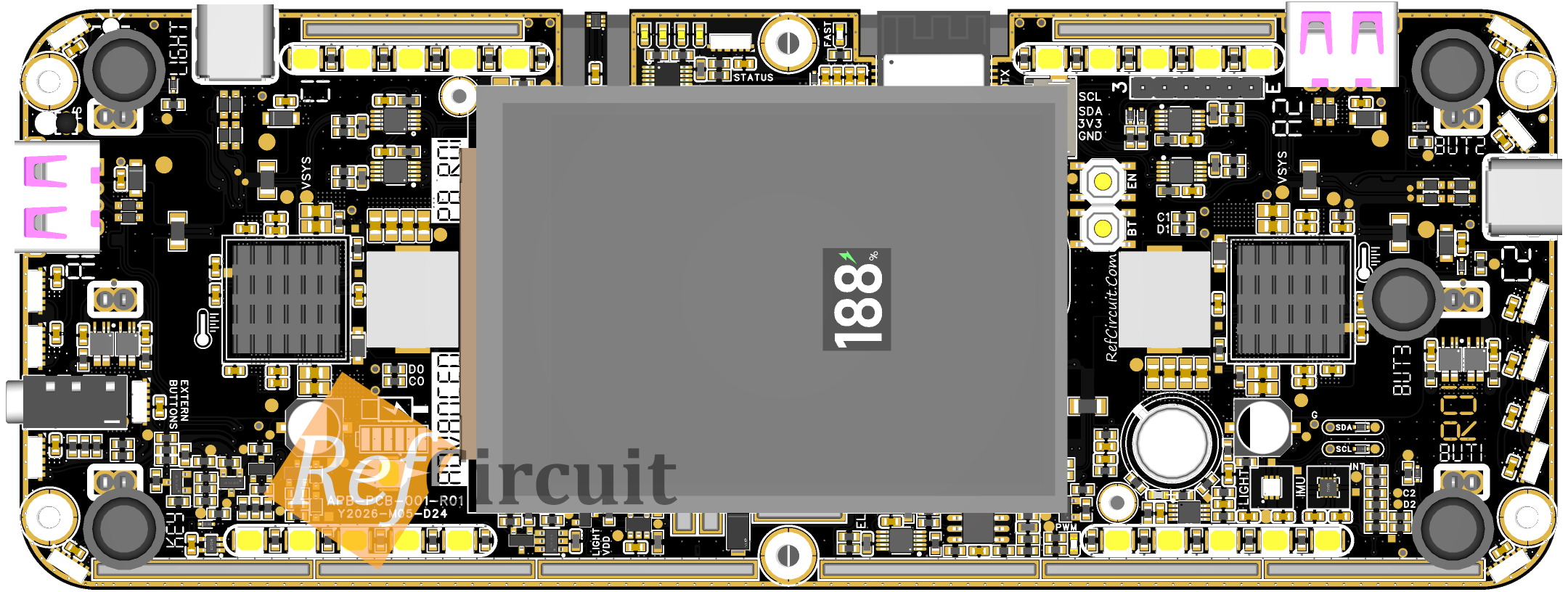
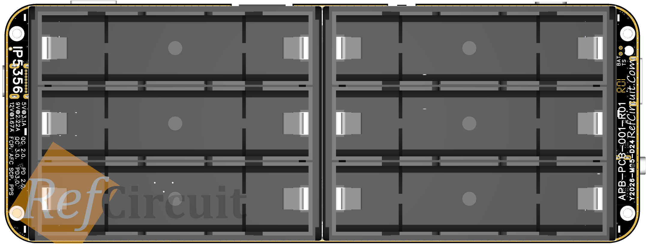
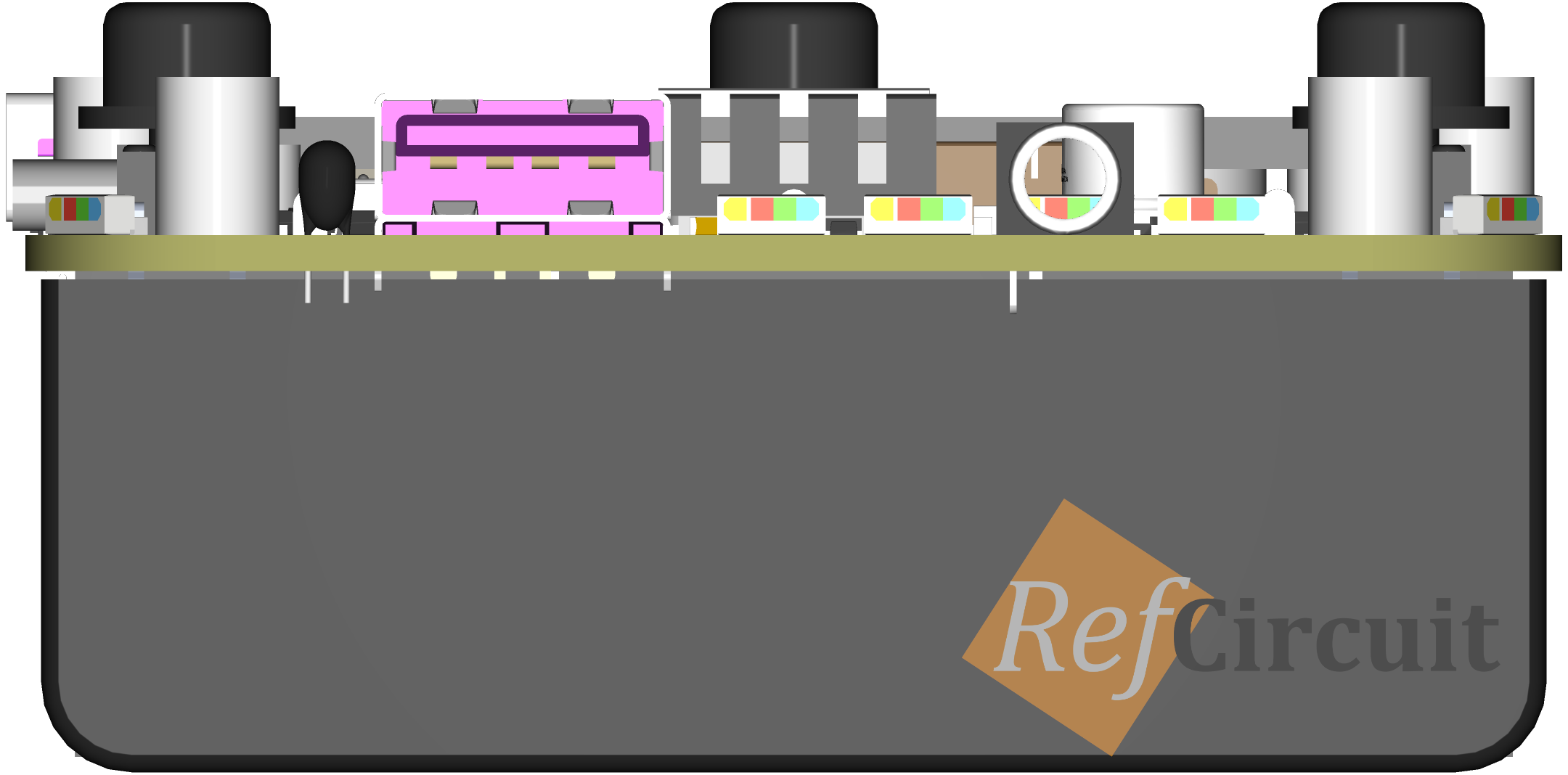
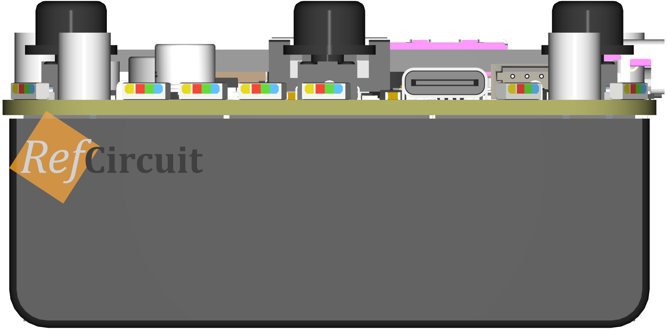
3D View
 |  |
 |  |
 |  |
Assembly
 |  |
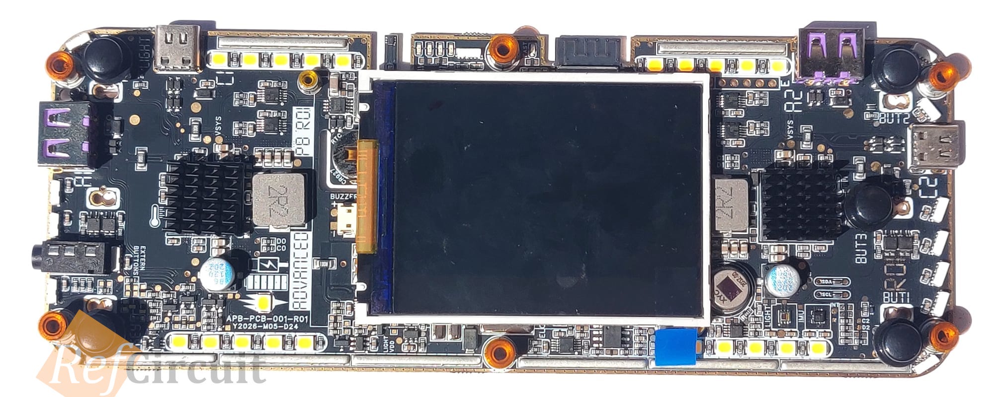
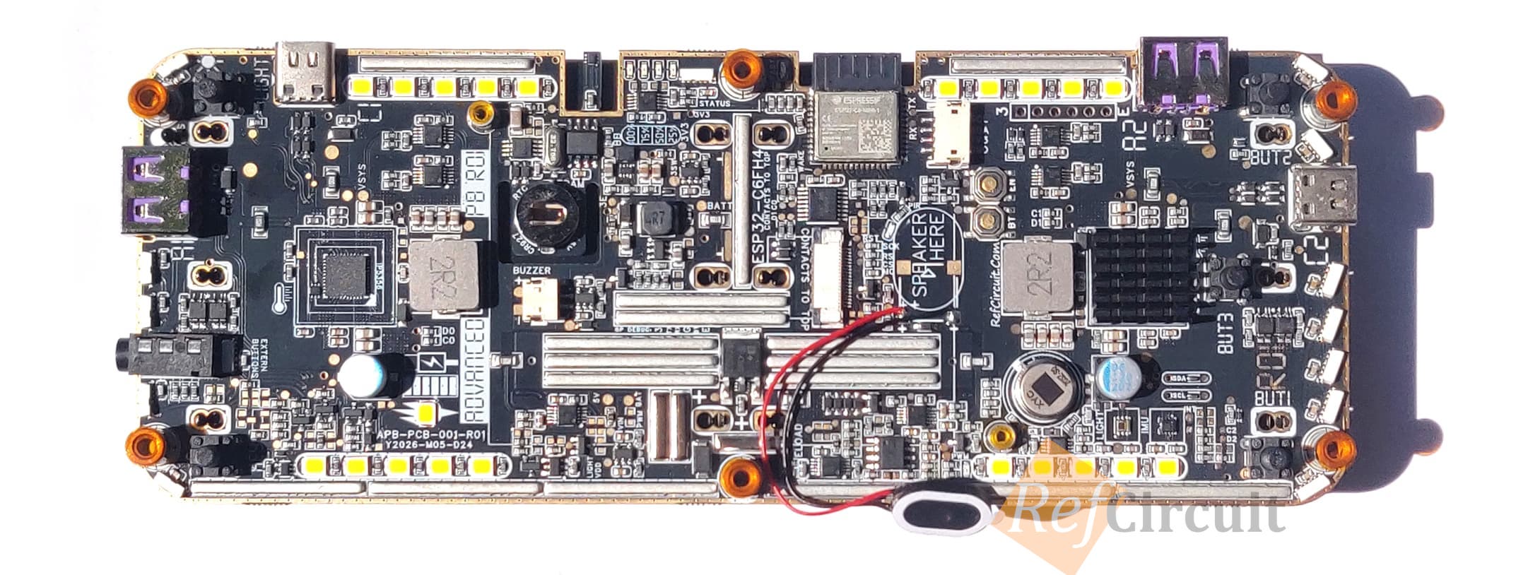
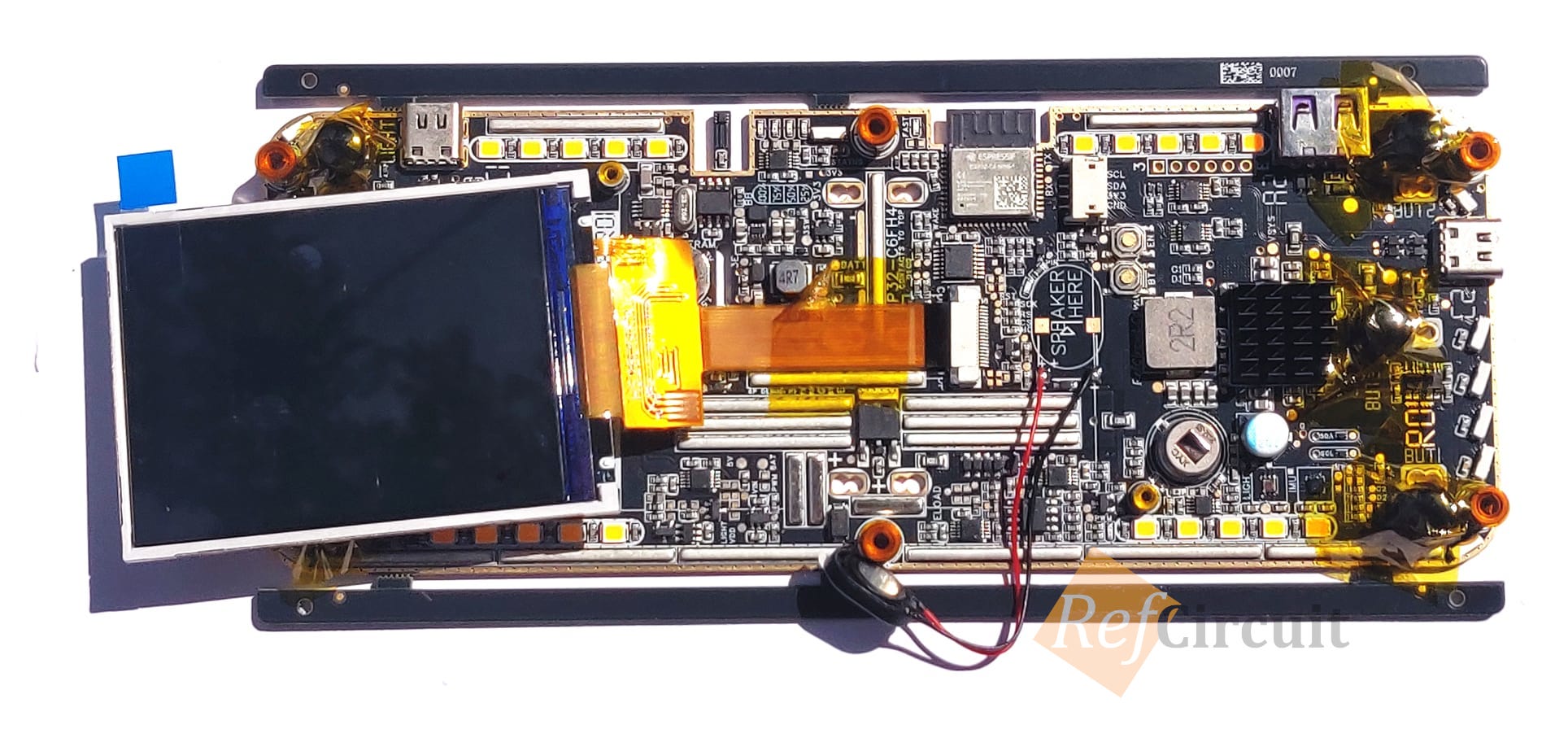
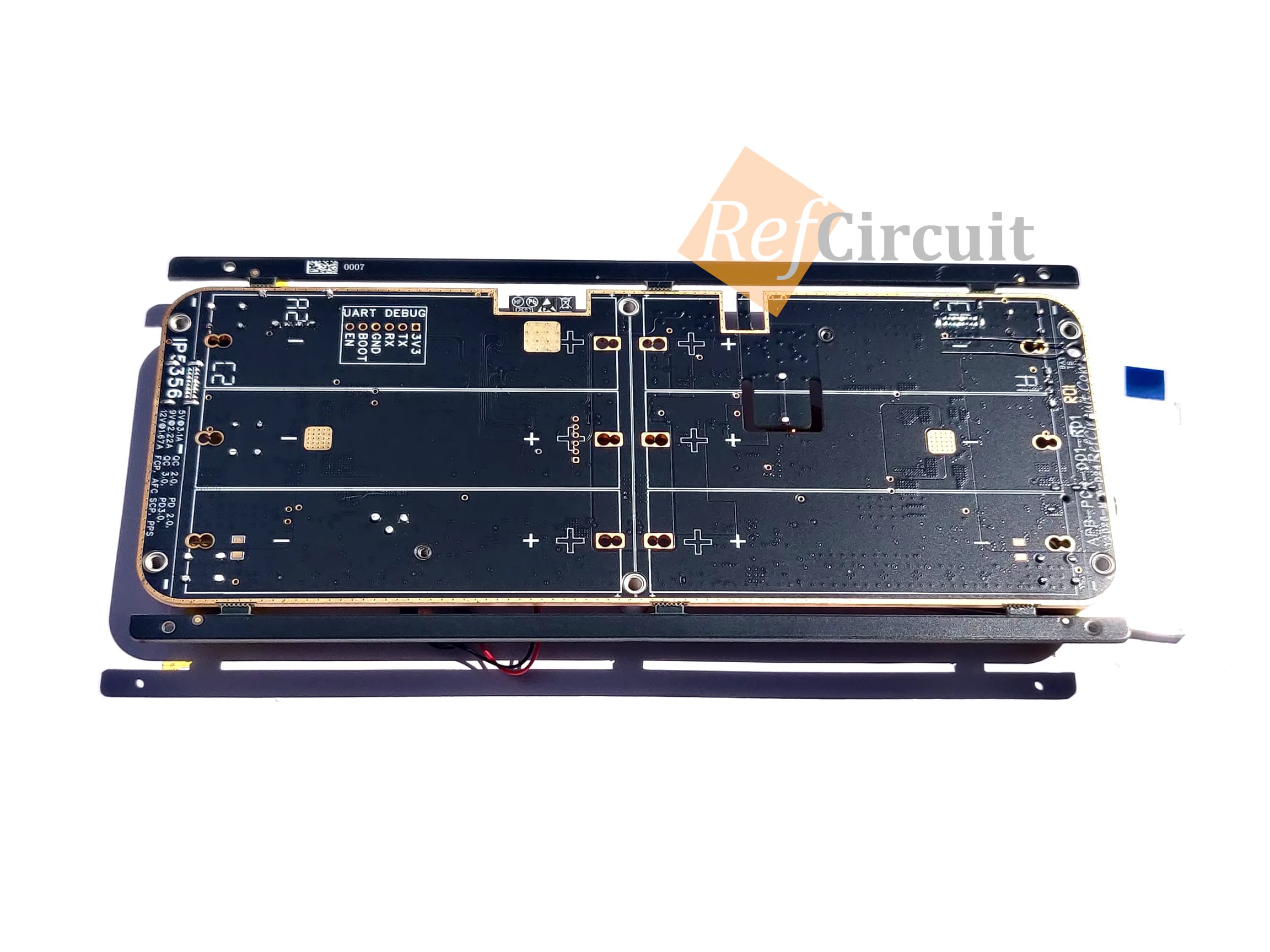
Acceptance
 | |
 |  |
 |  |
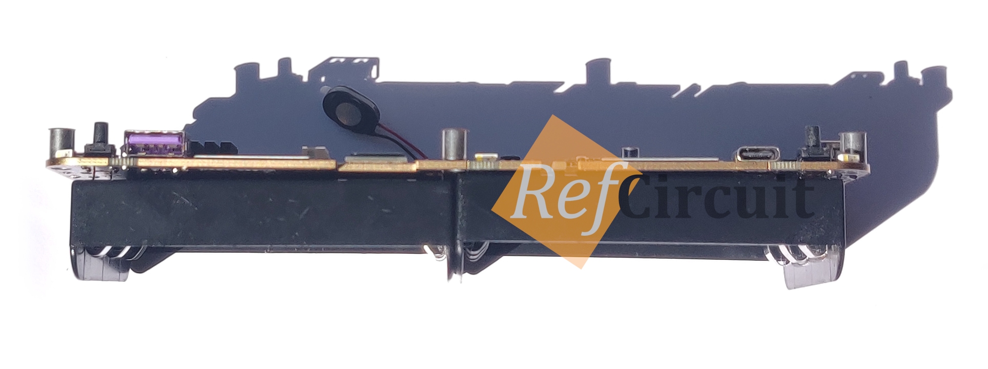 | 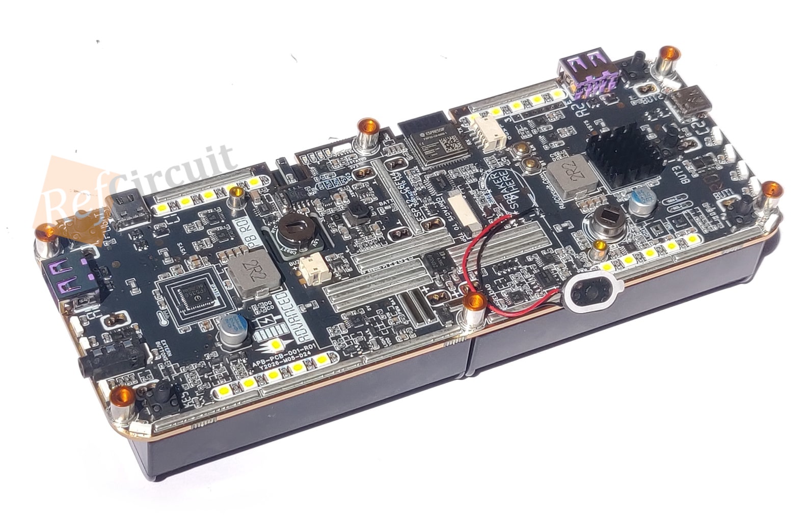 |
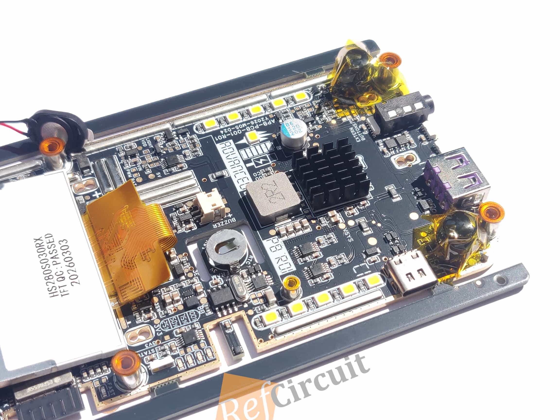 | 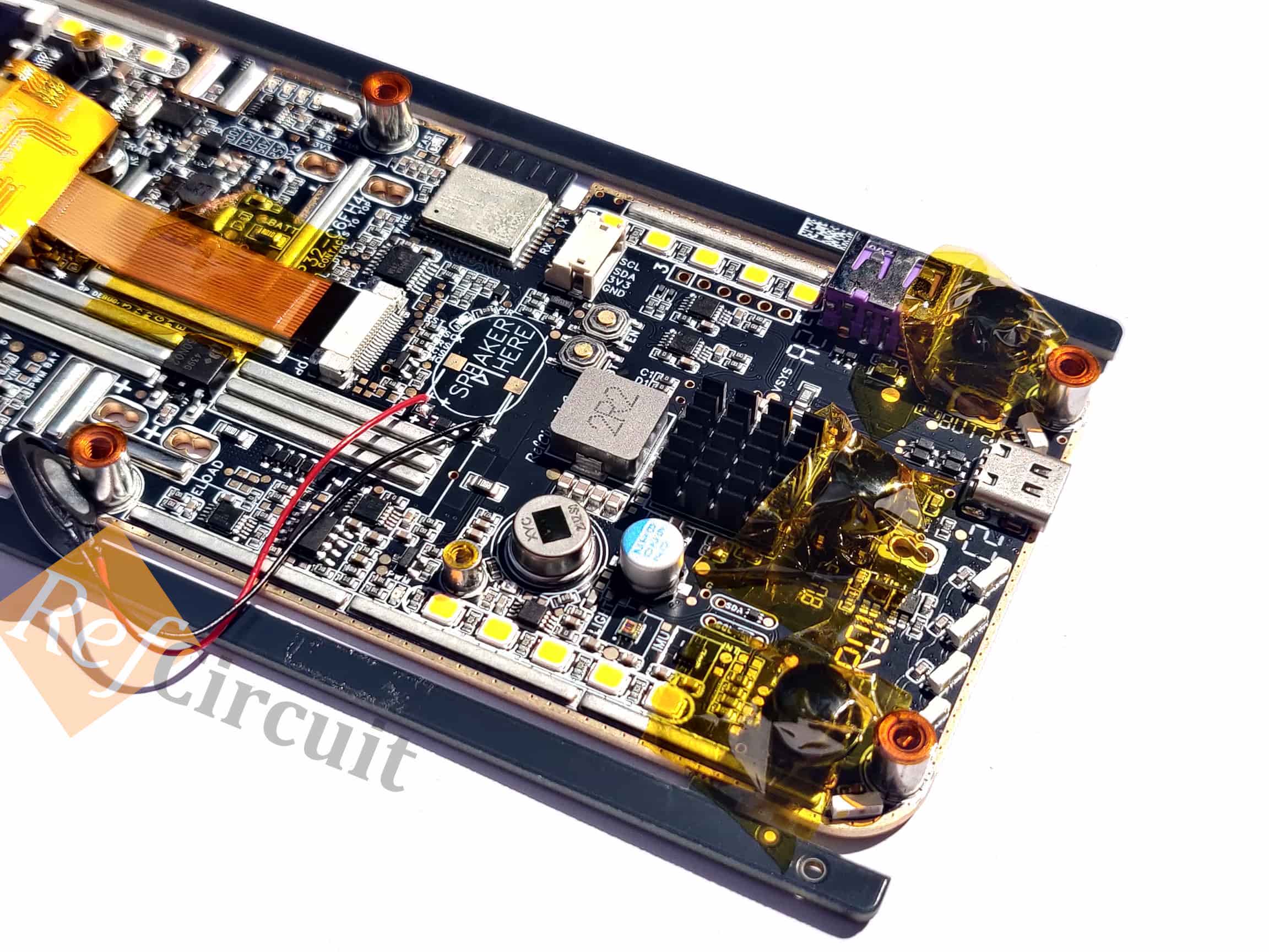 |
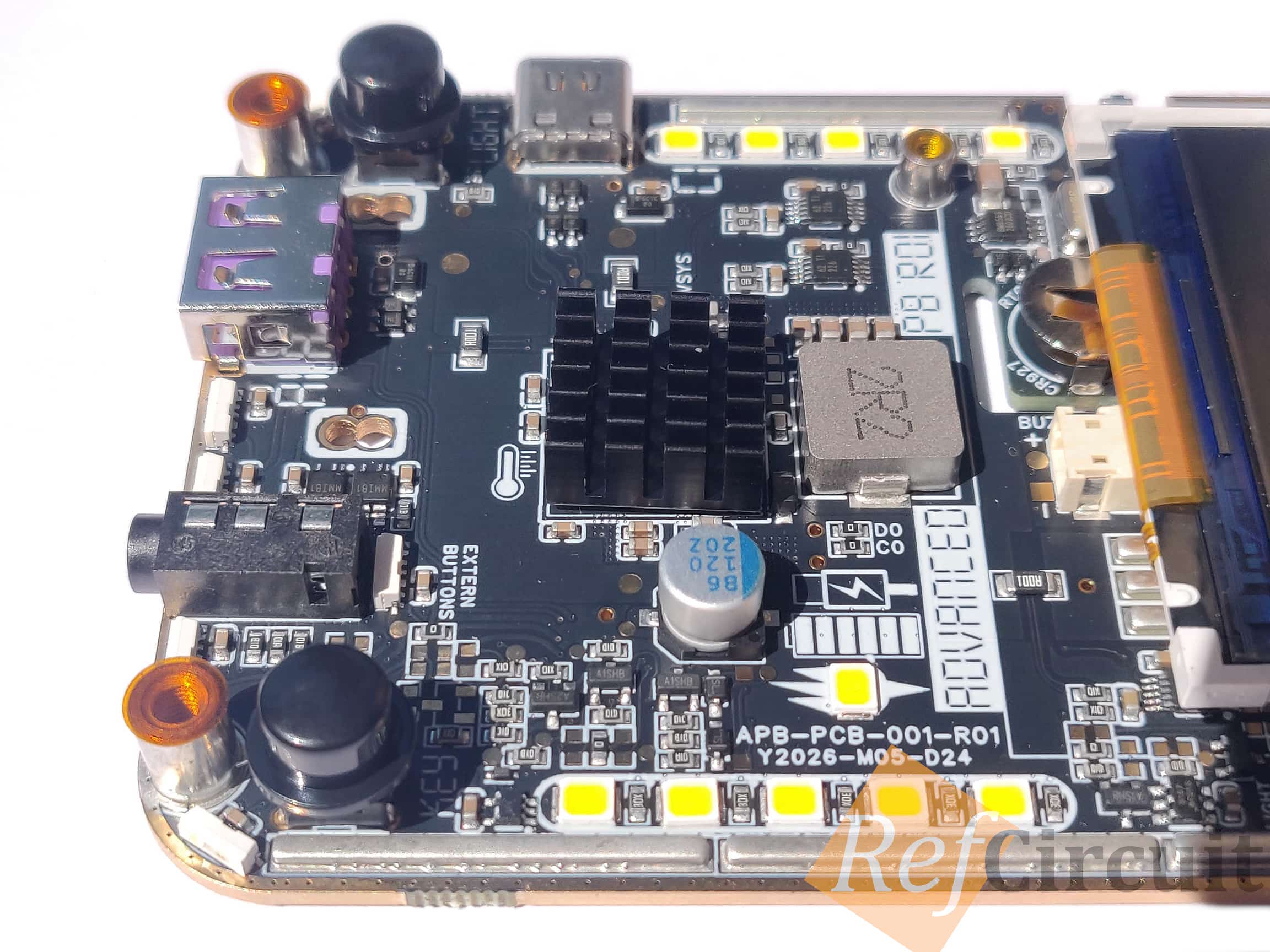 | 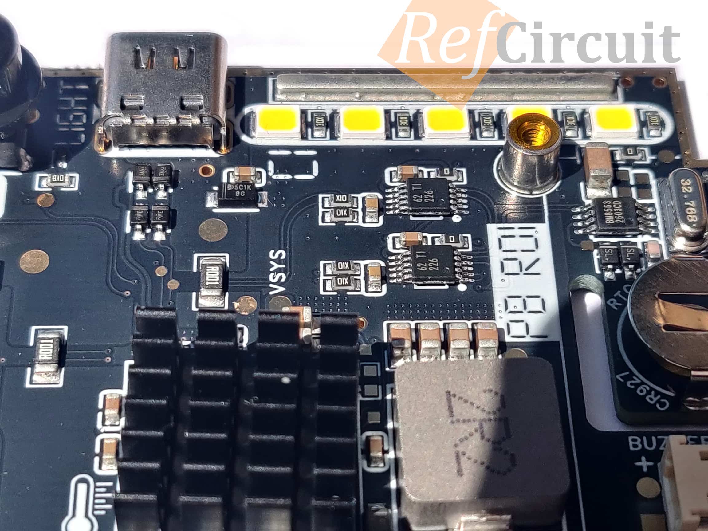 |
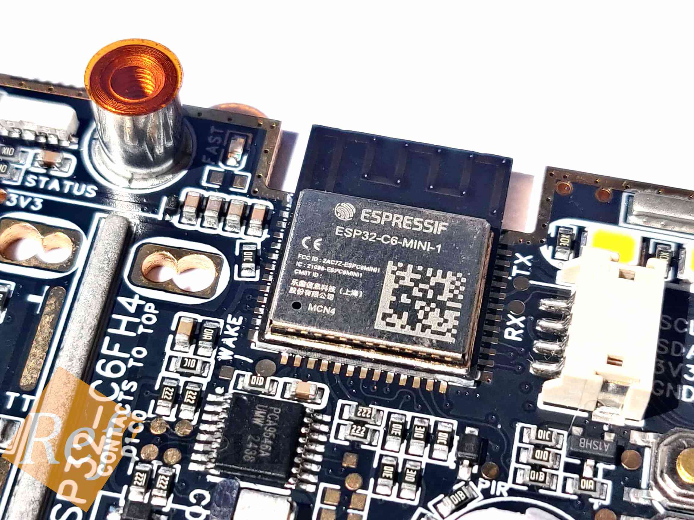 | 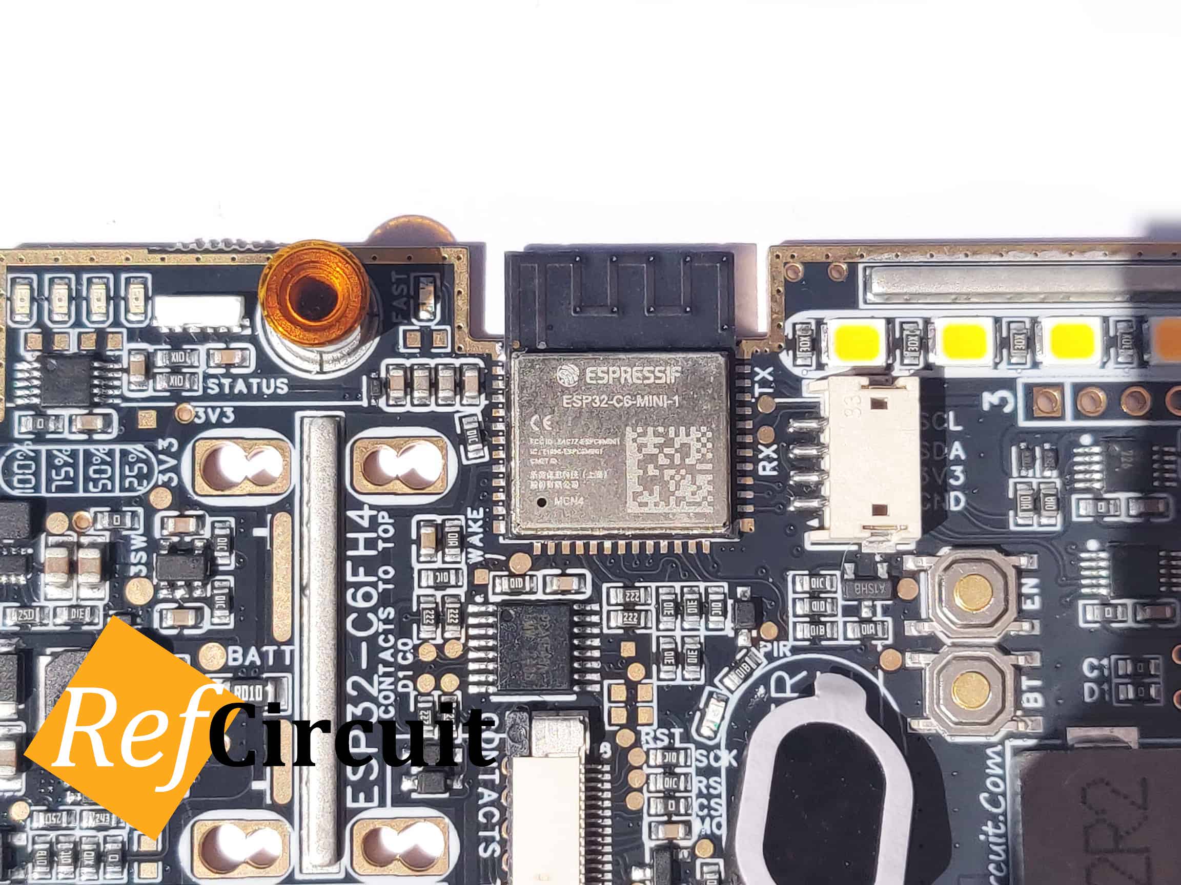 |
 |  |
 |  |
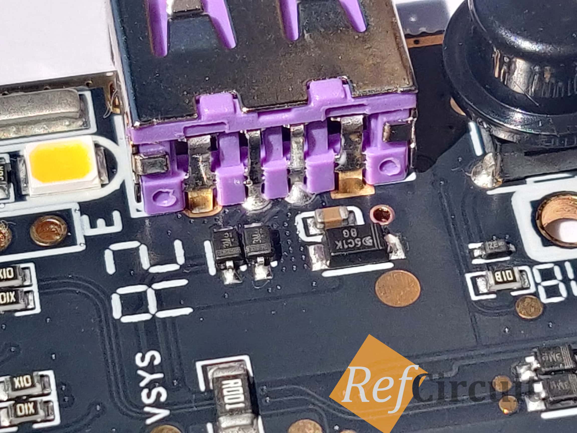 | 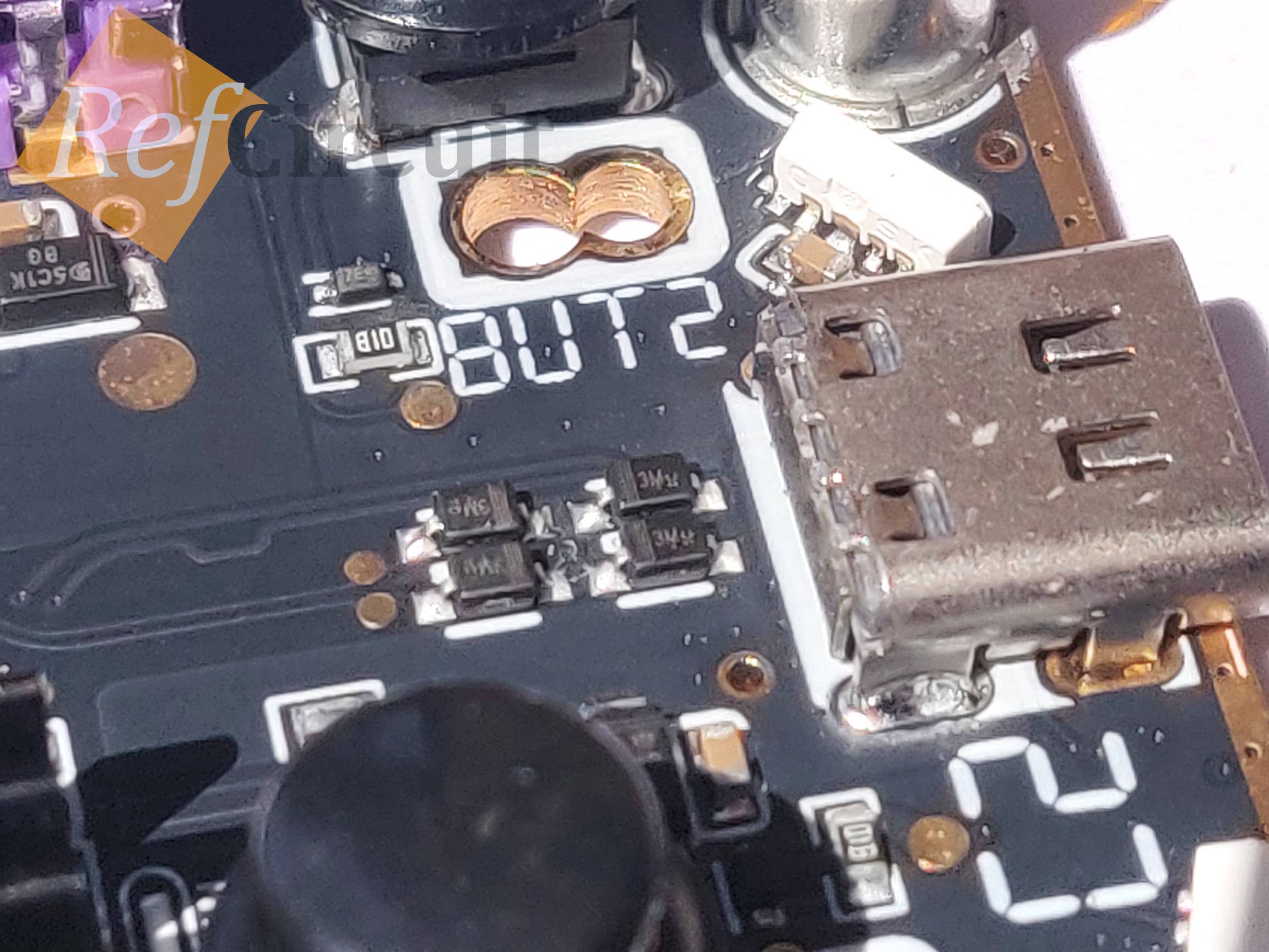 |
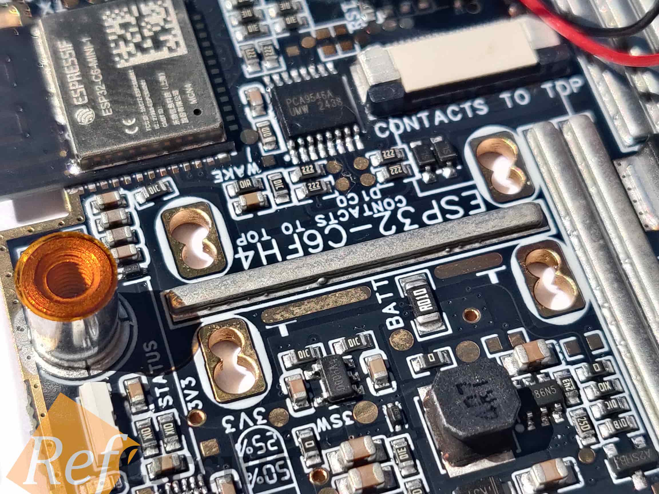 | 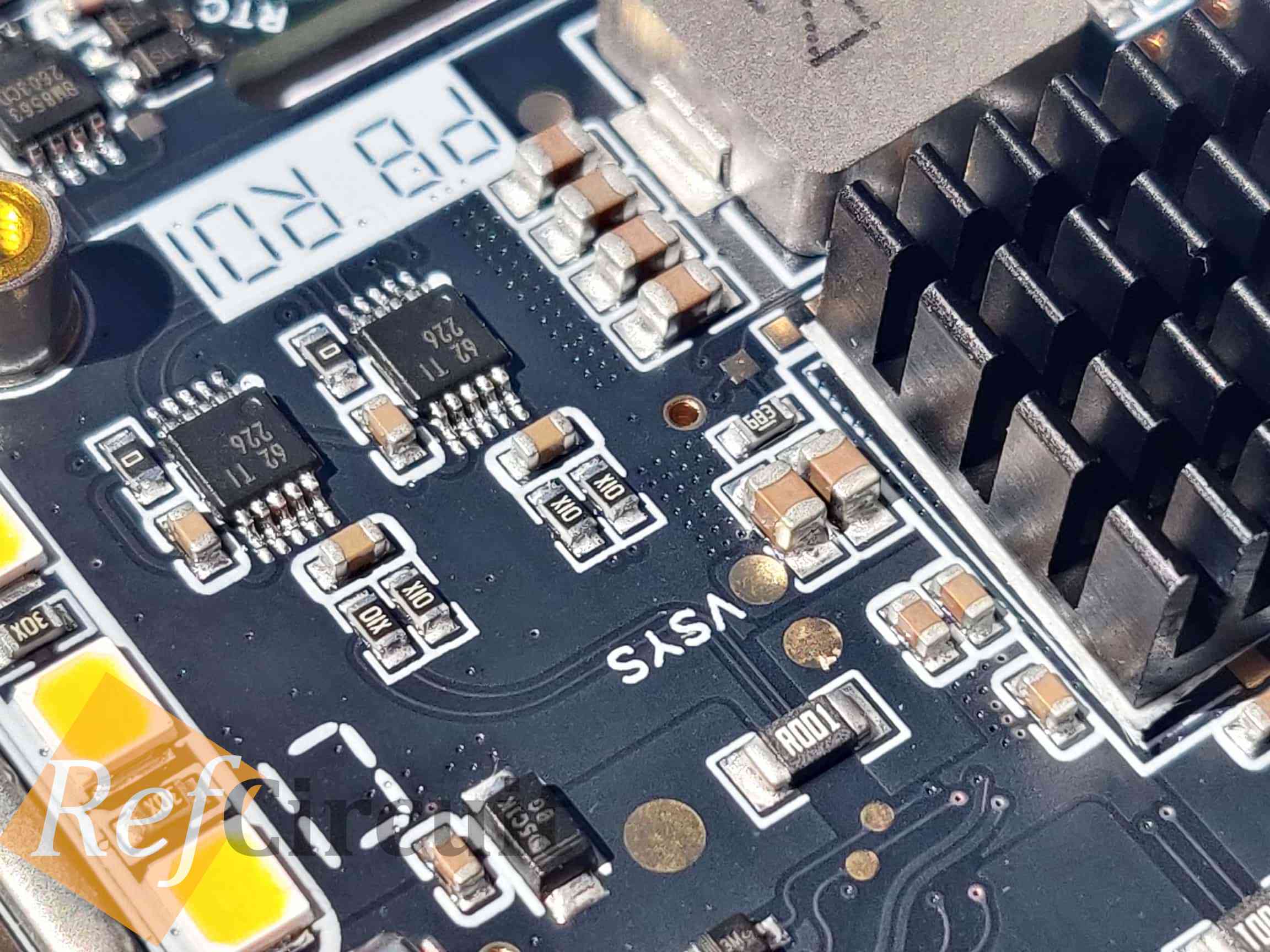 |
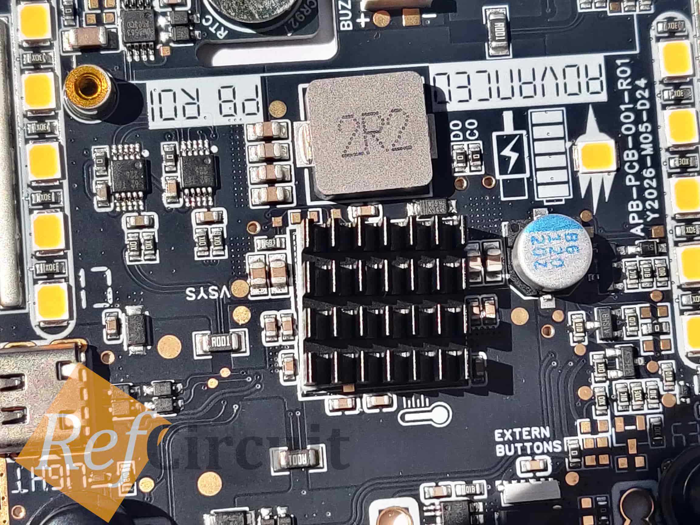 | 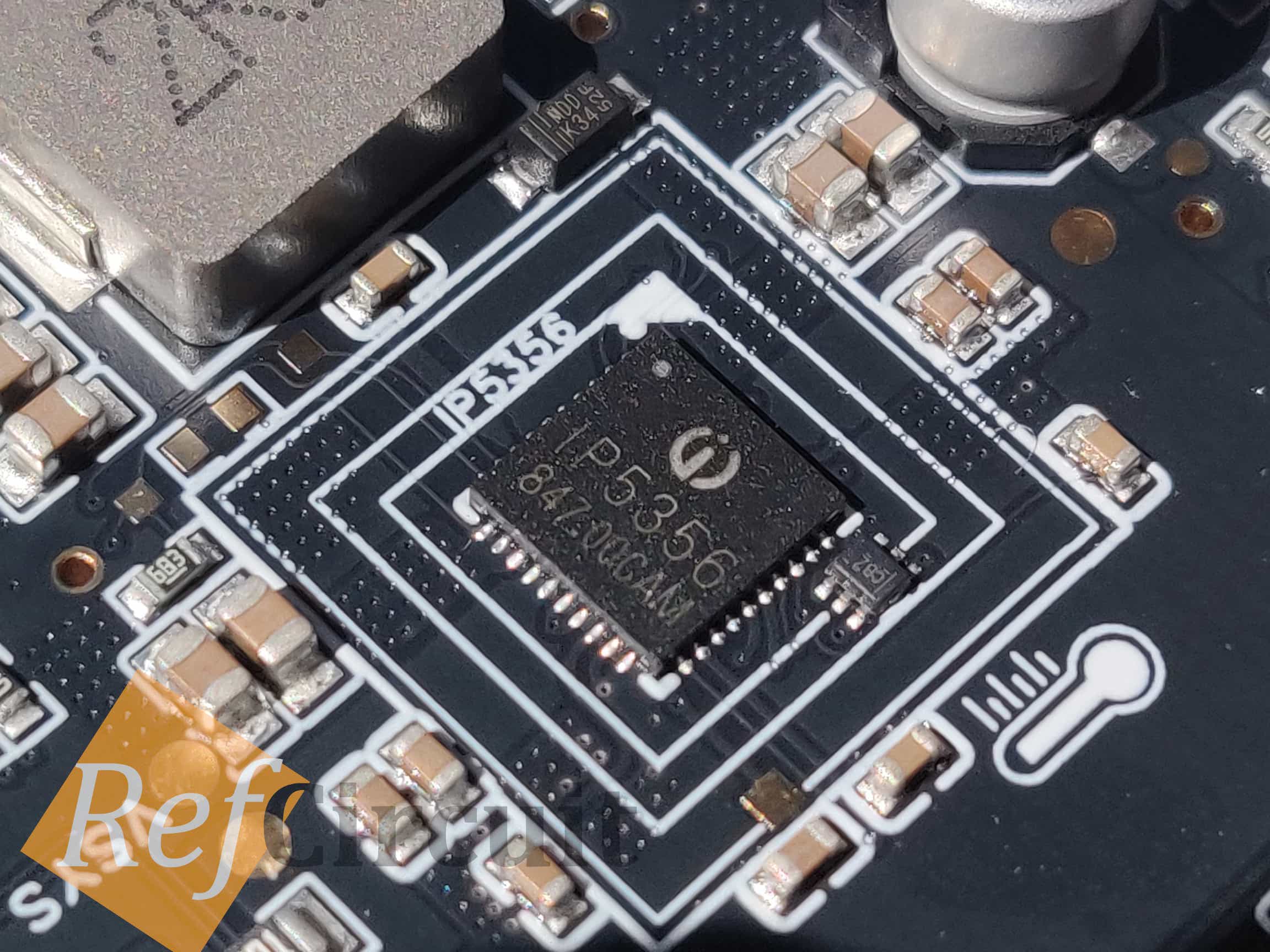 |
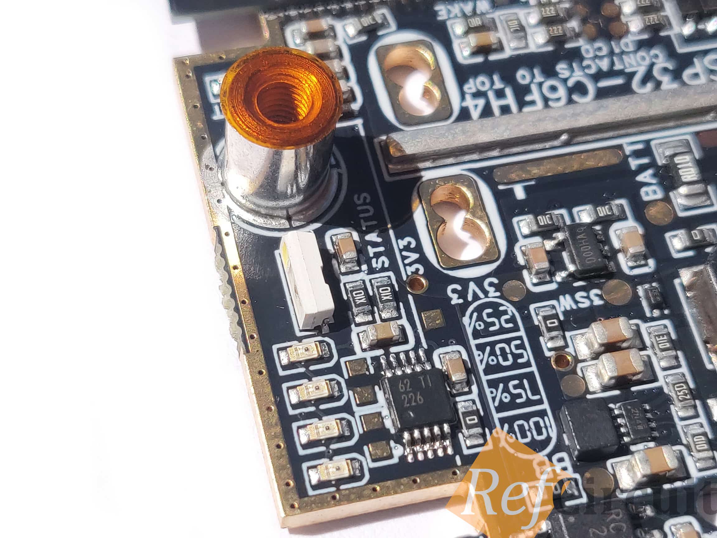 | 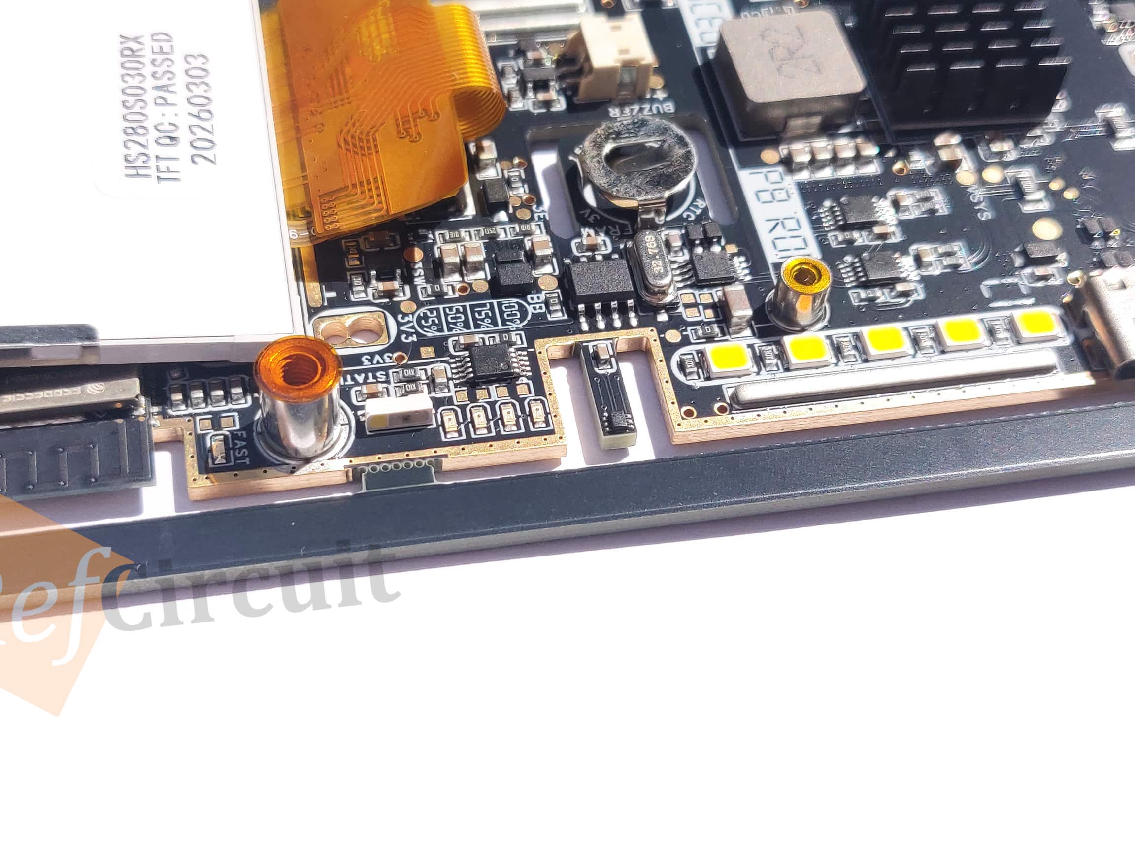 |
 |  |
 |  |
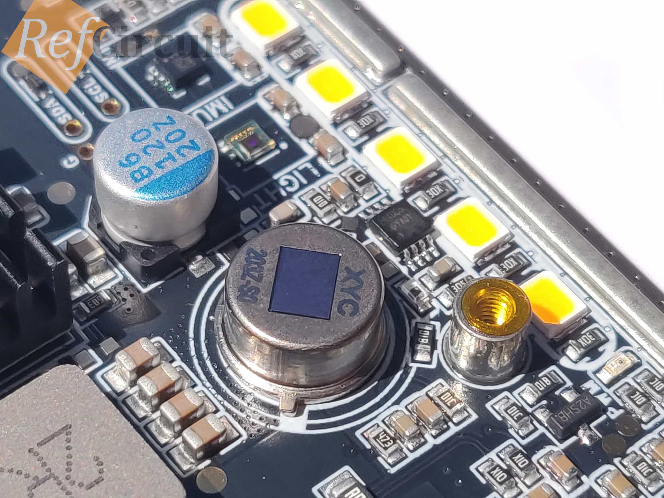 | 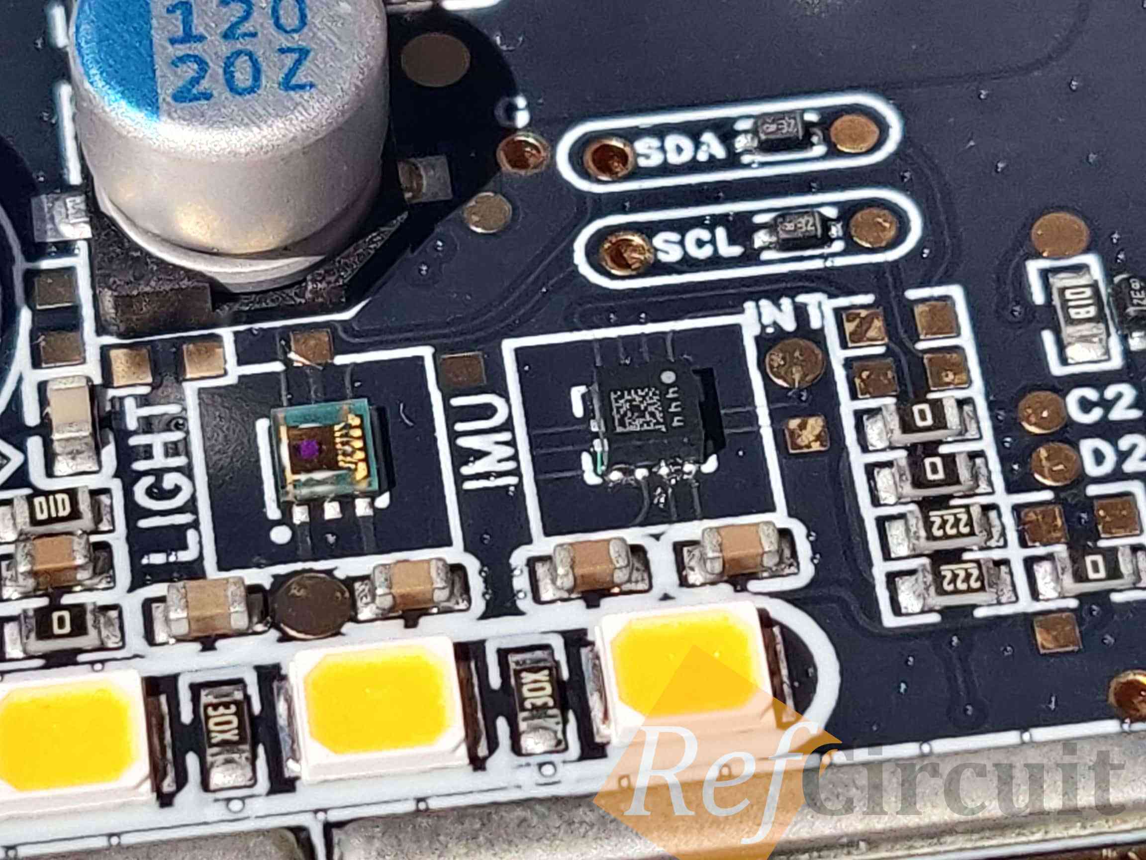 |
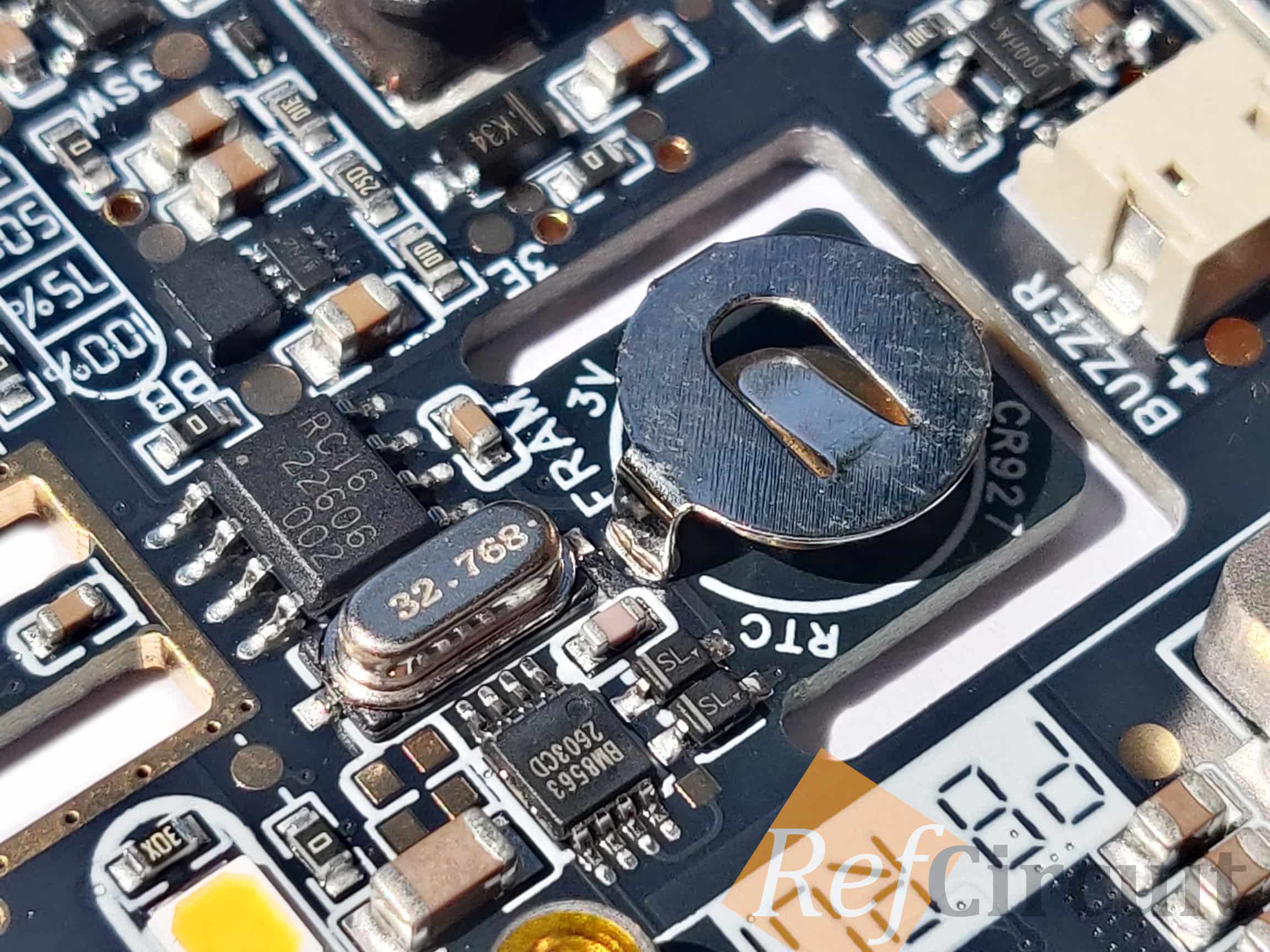 | 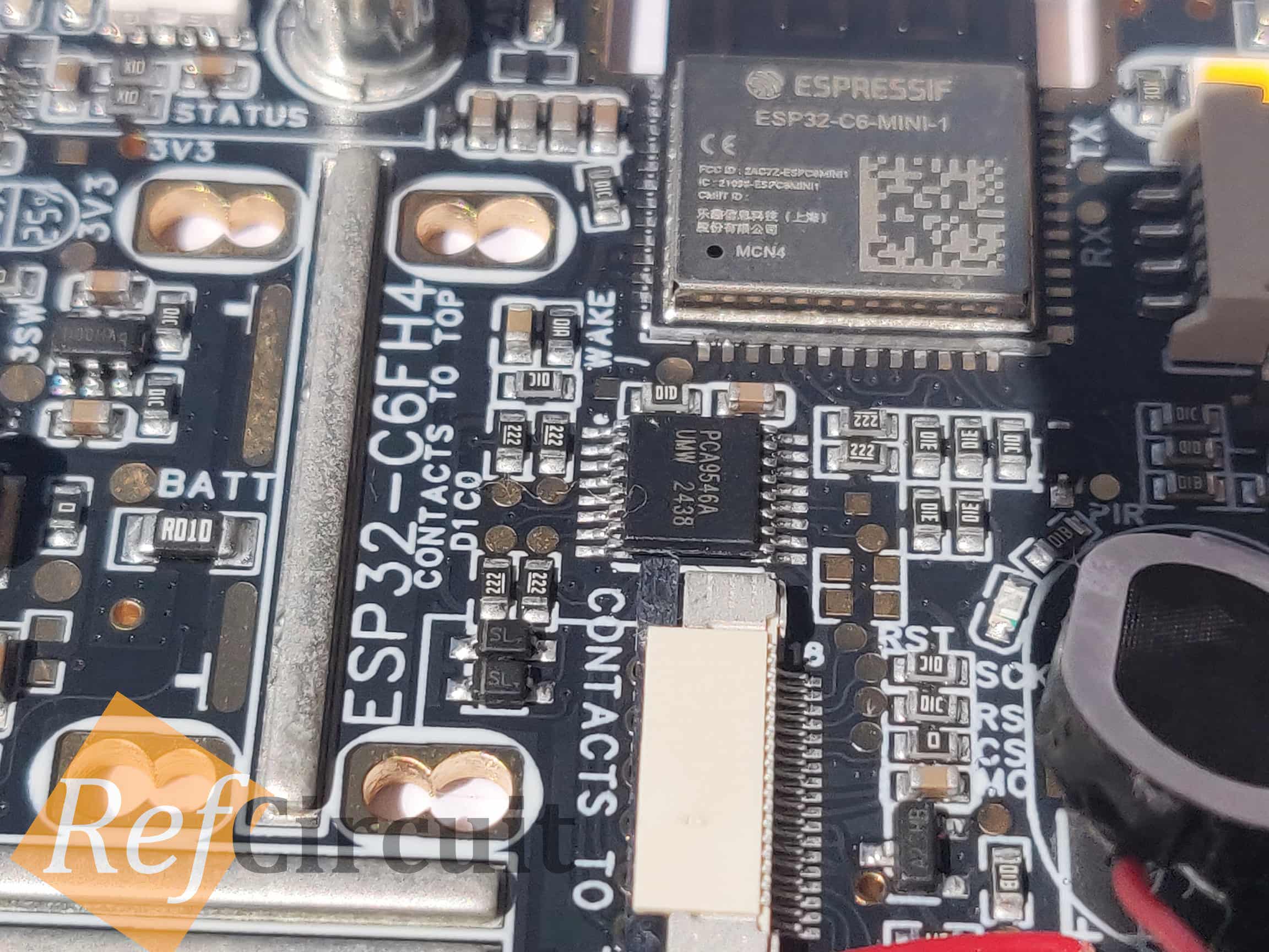 |
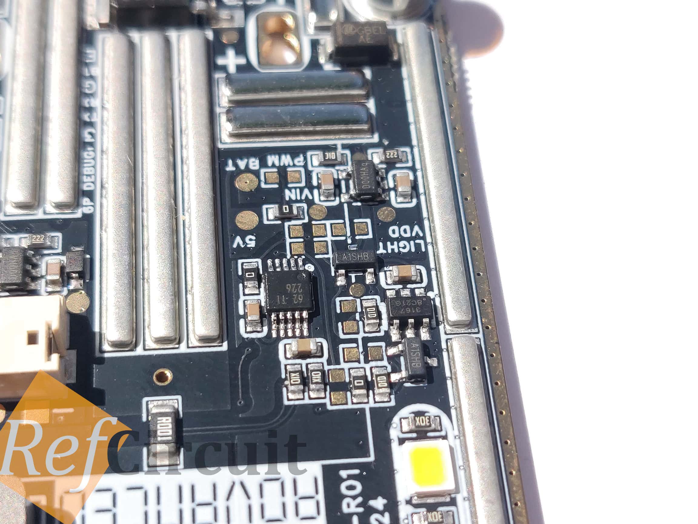 | 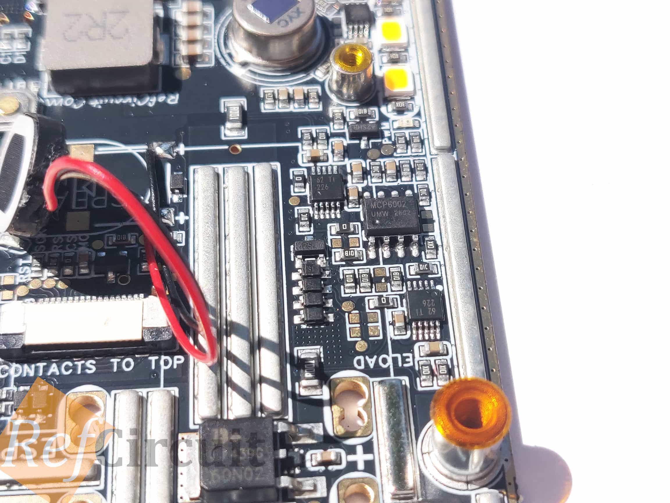 |
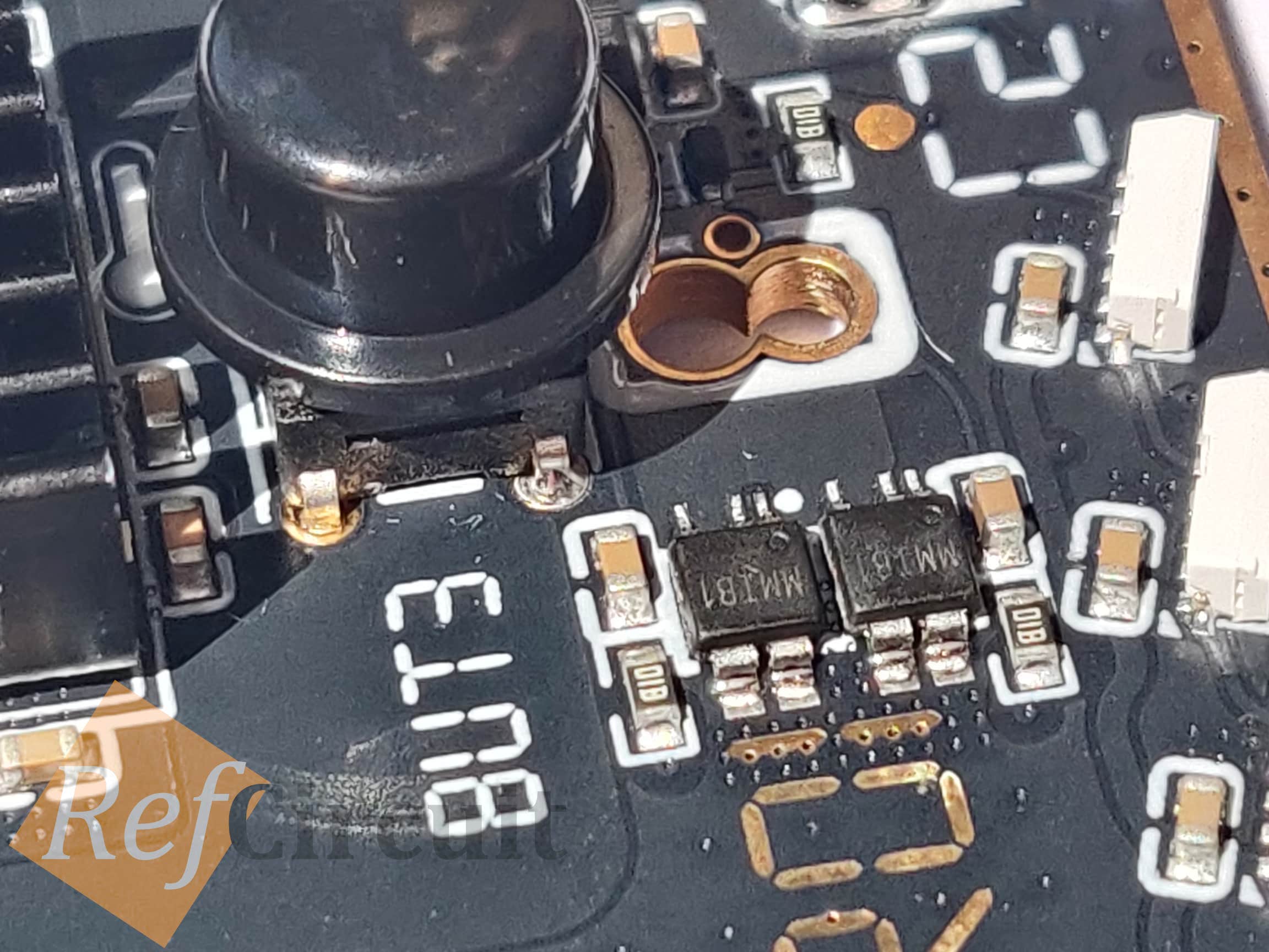 | 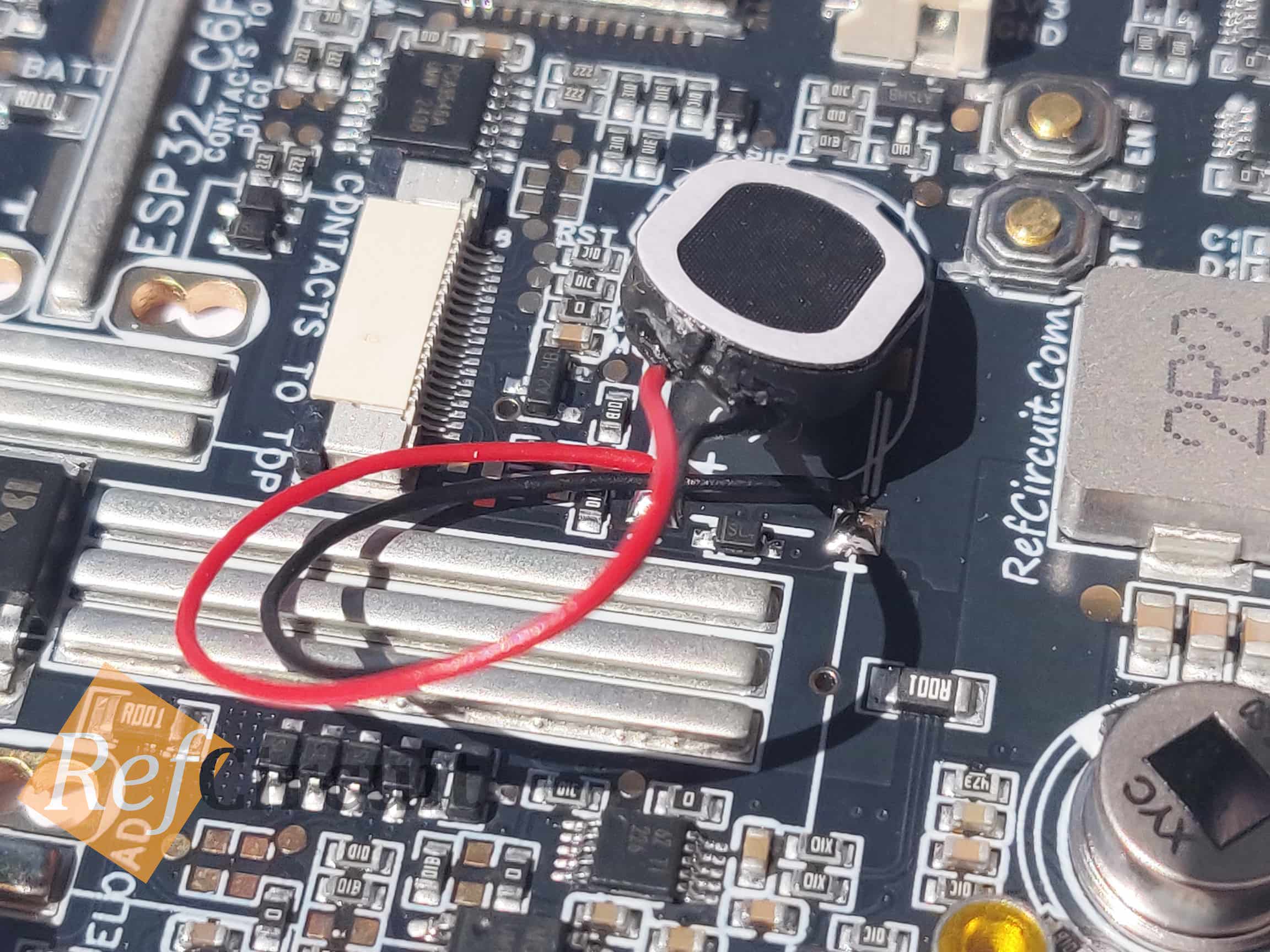 |
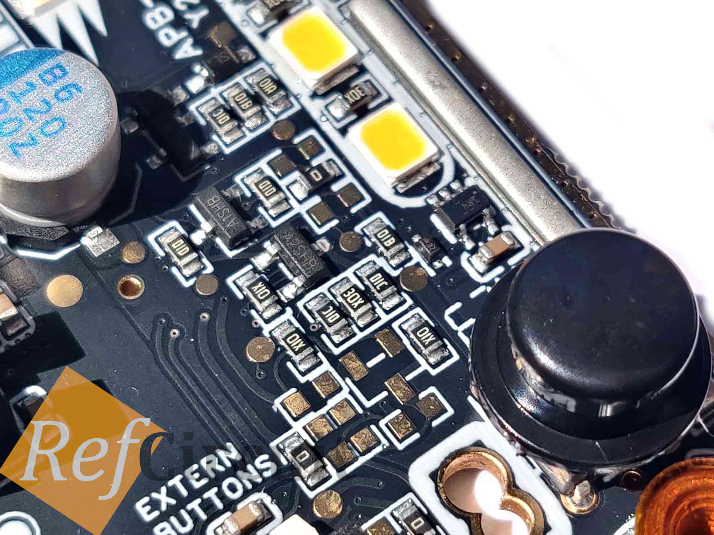 | 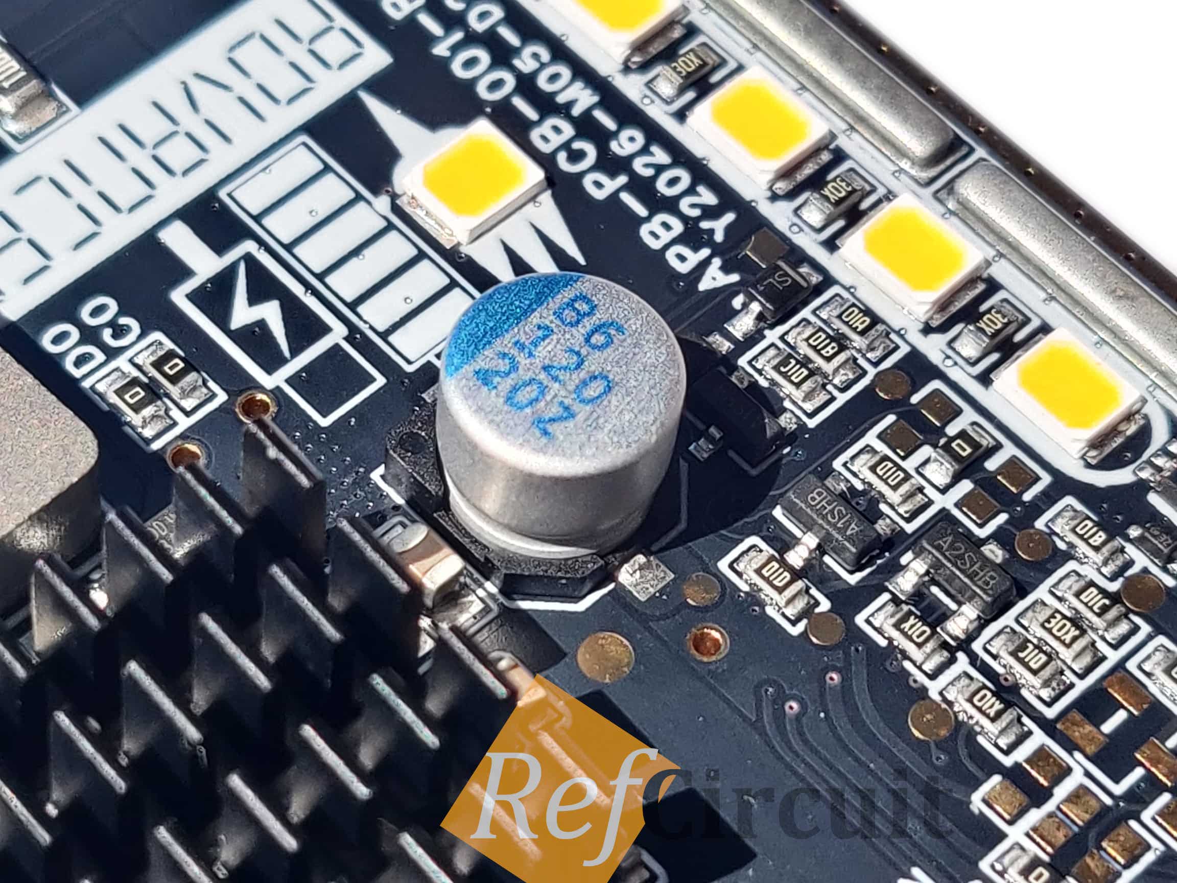 |
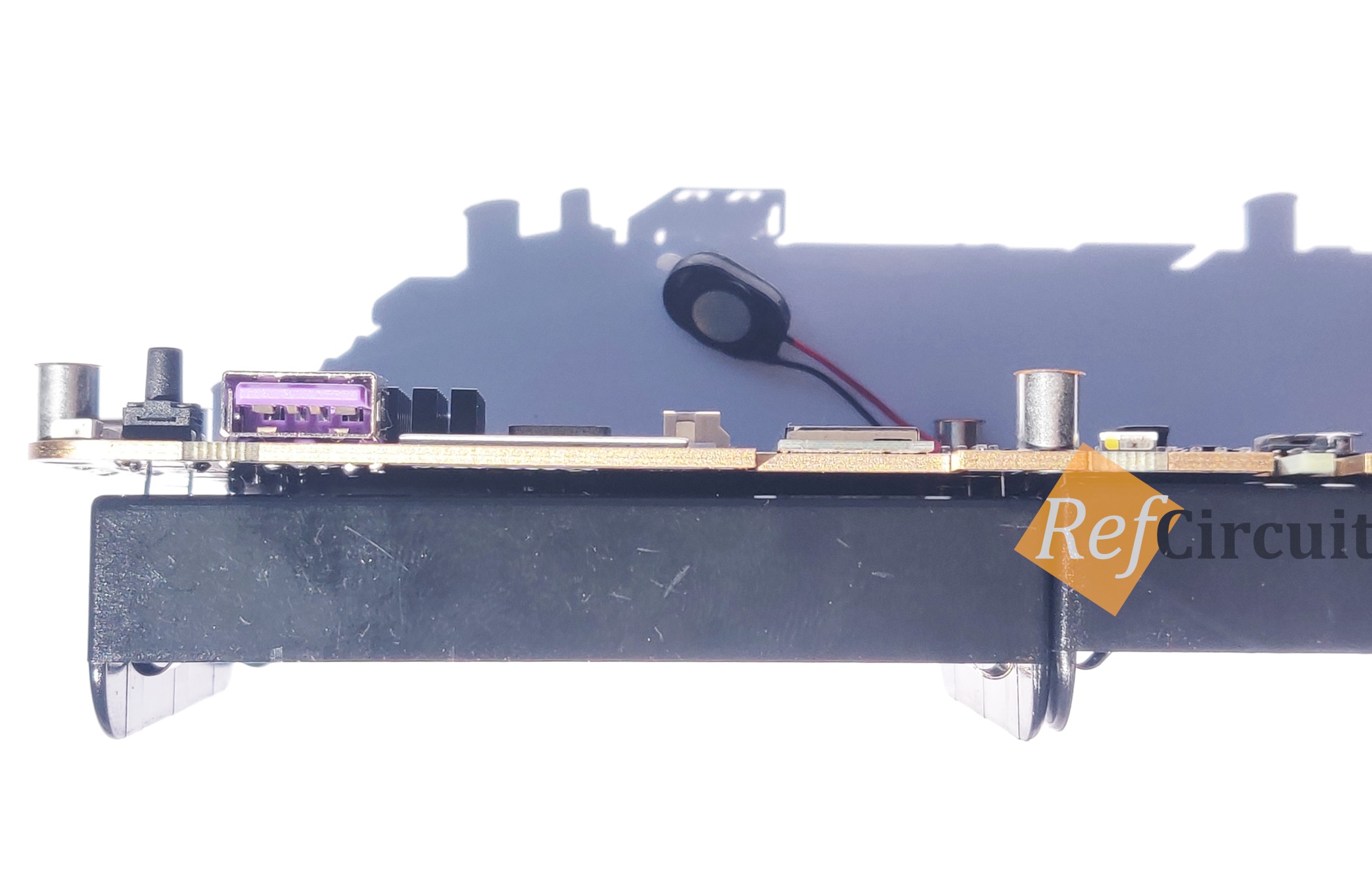 | 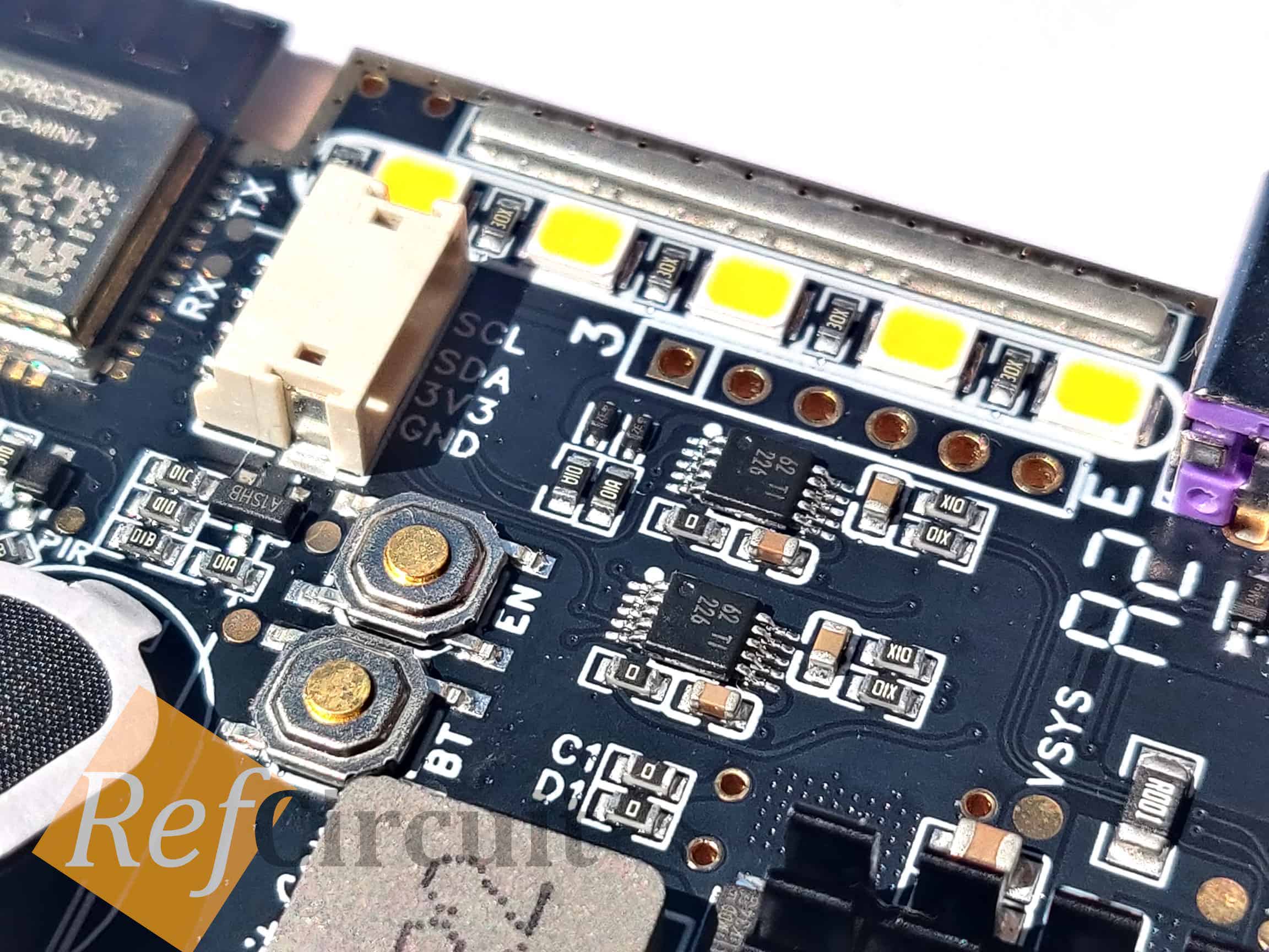 |
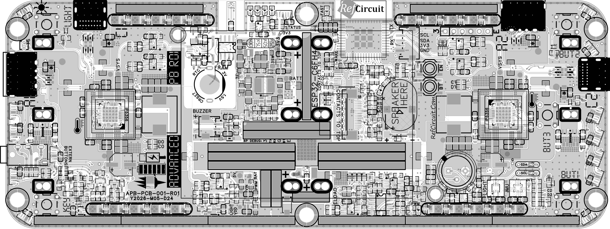
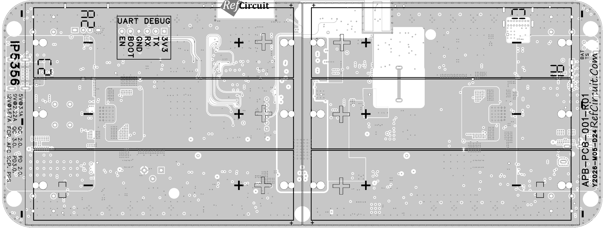
Layout
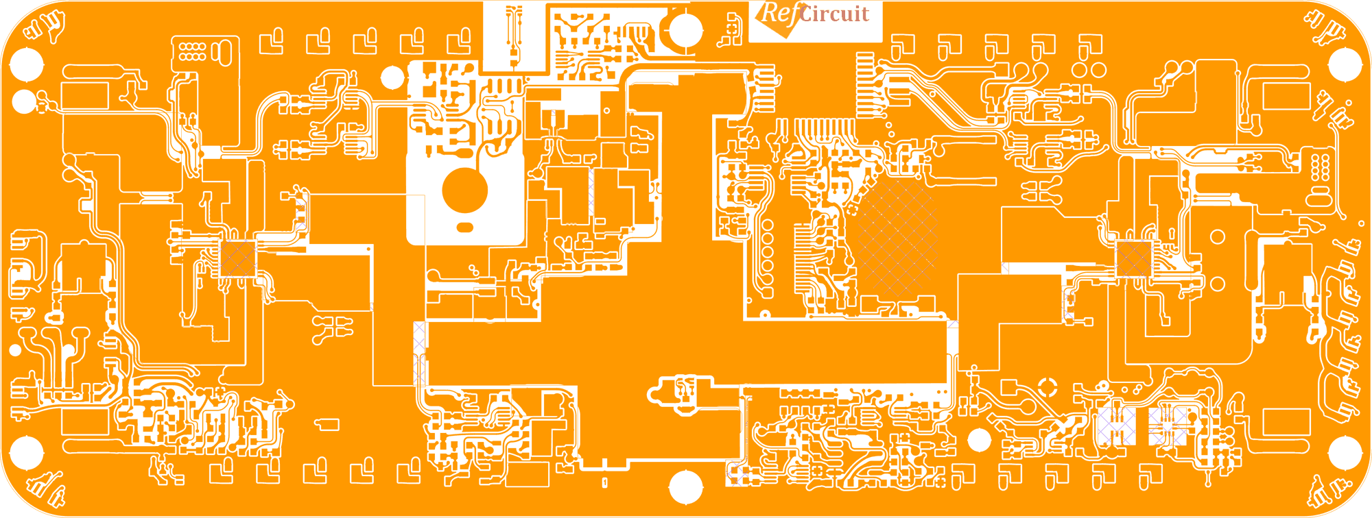 | 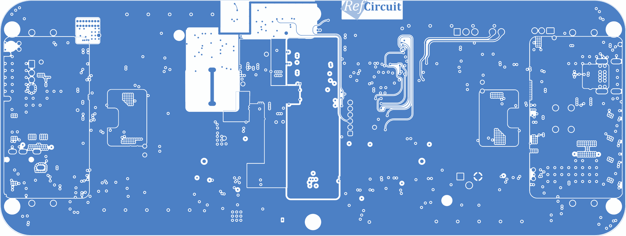 |
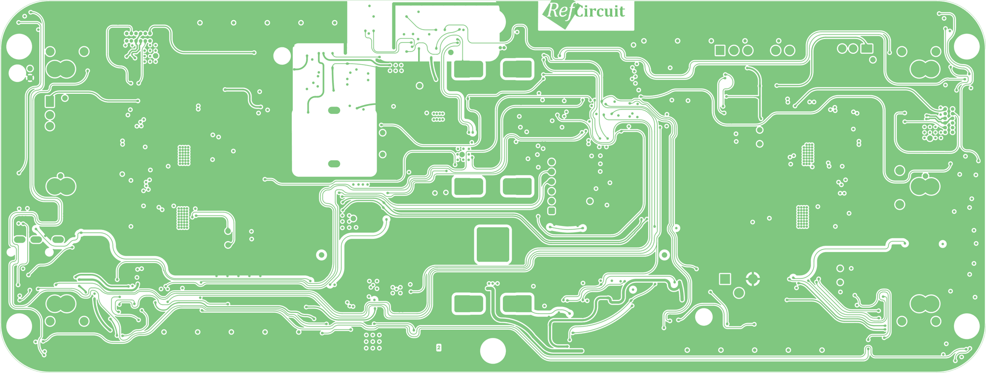 | 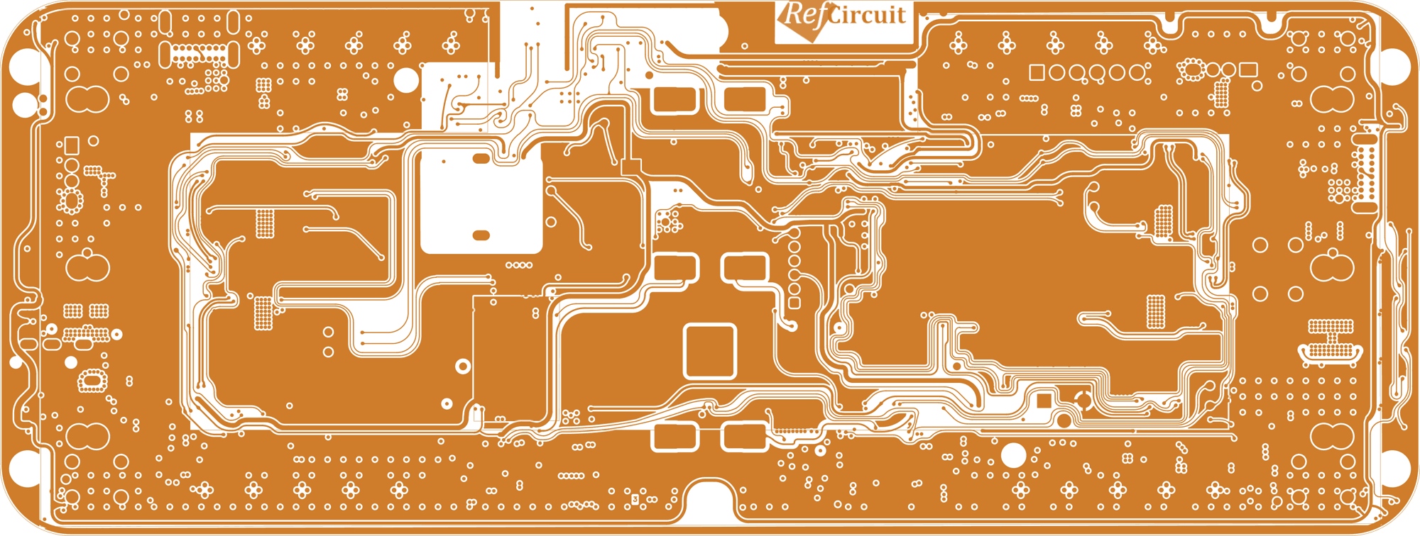 |
Remarks
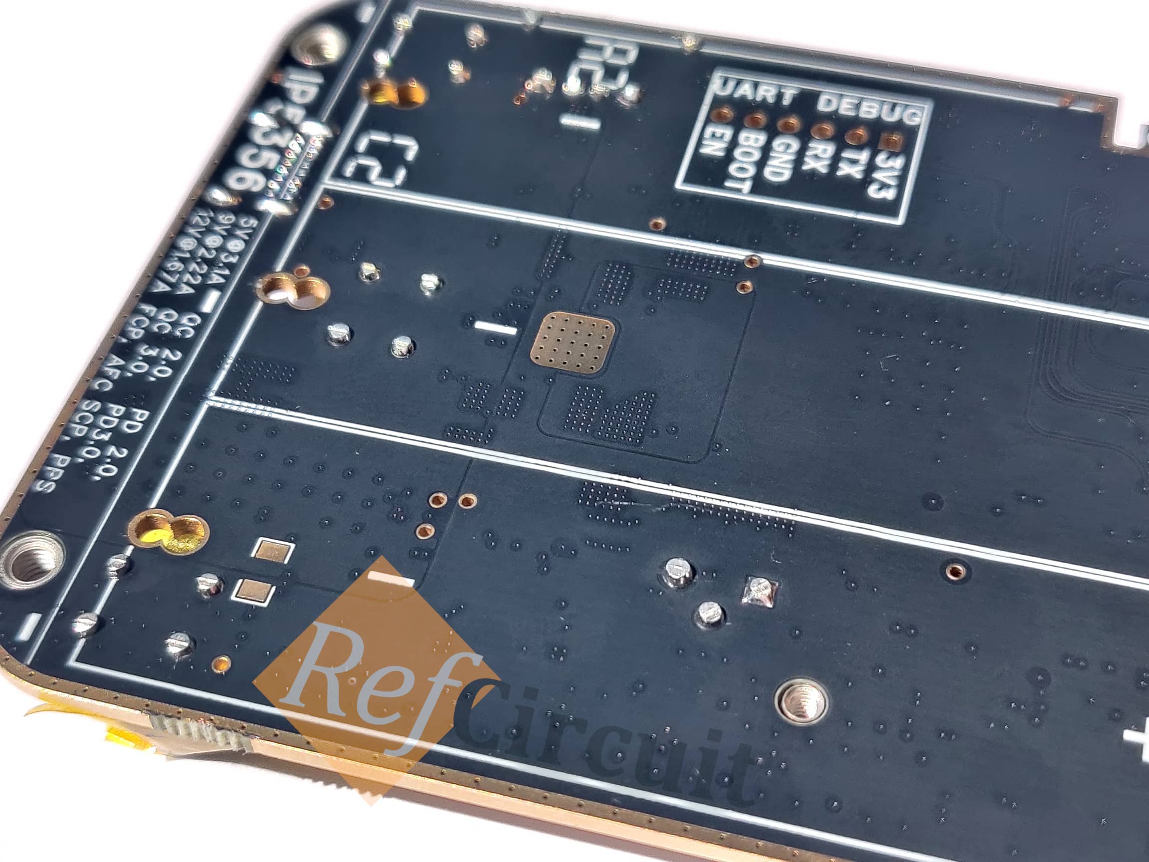
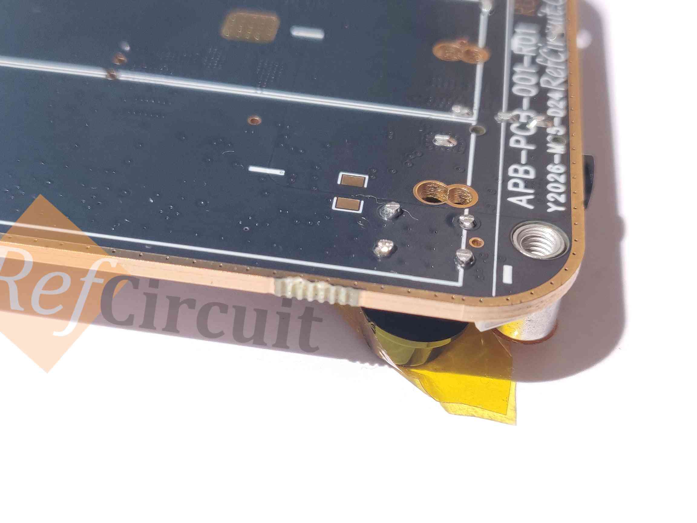
- CUTOFF ALL THT PINS ON BOTTOM SIDE
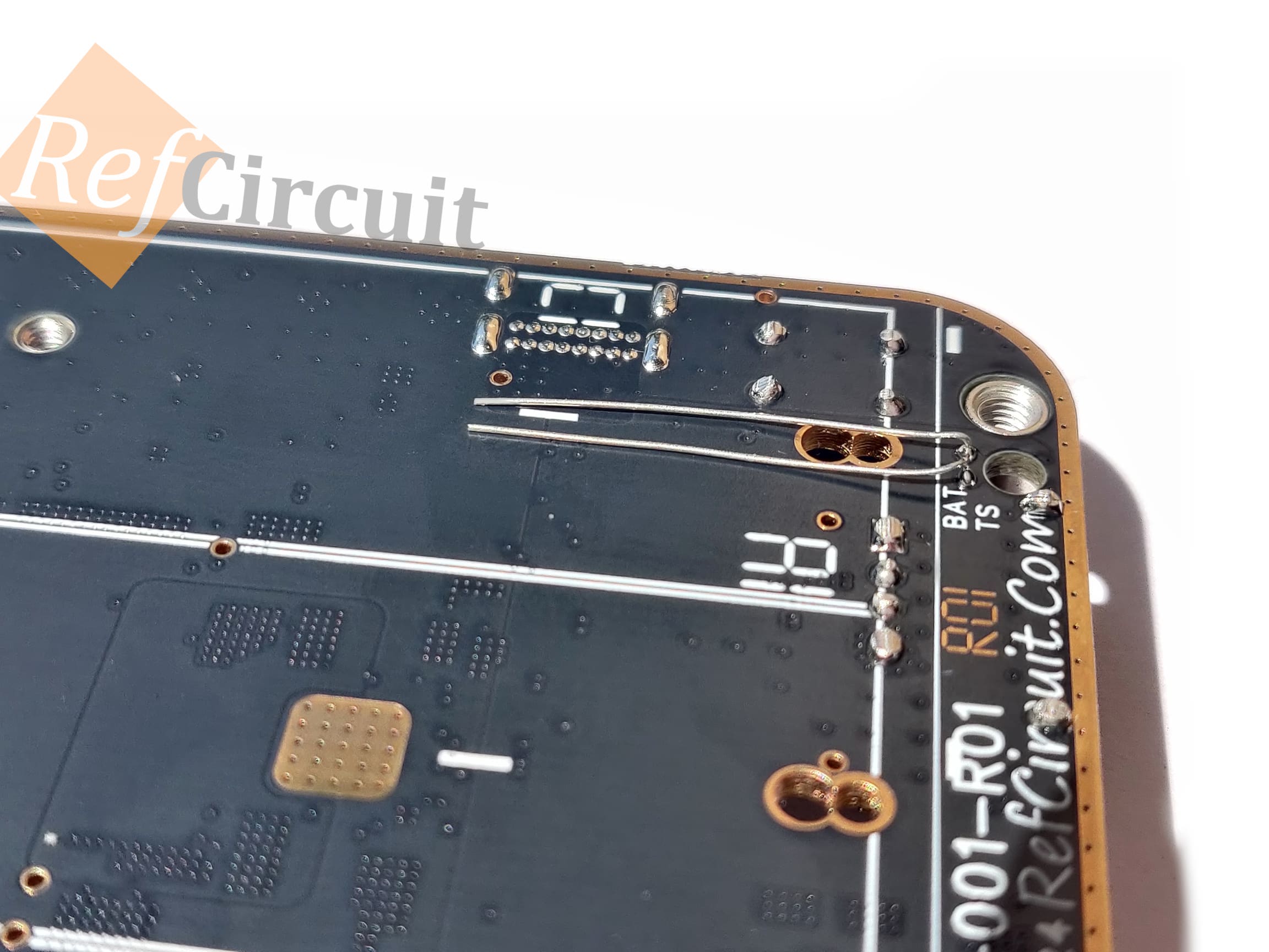
- DO NOT REDUCE (CUT) THE LENGTH OF THE NTC TS LEAD
- INSERT CAPS ONTO BUTTONS
- PLACE HEATSINK ON THE TOP SIDE OF IC
- USE EDGE PLATING IF POSSIBLE
Soldering Issues
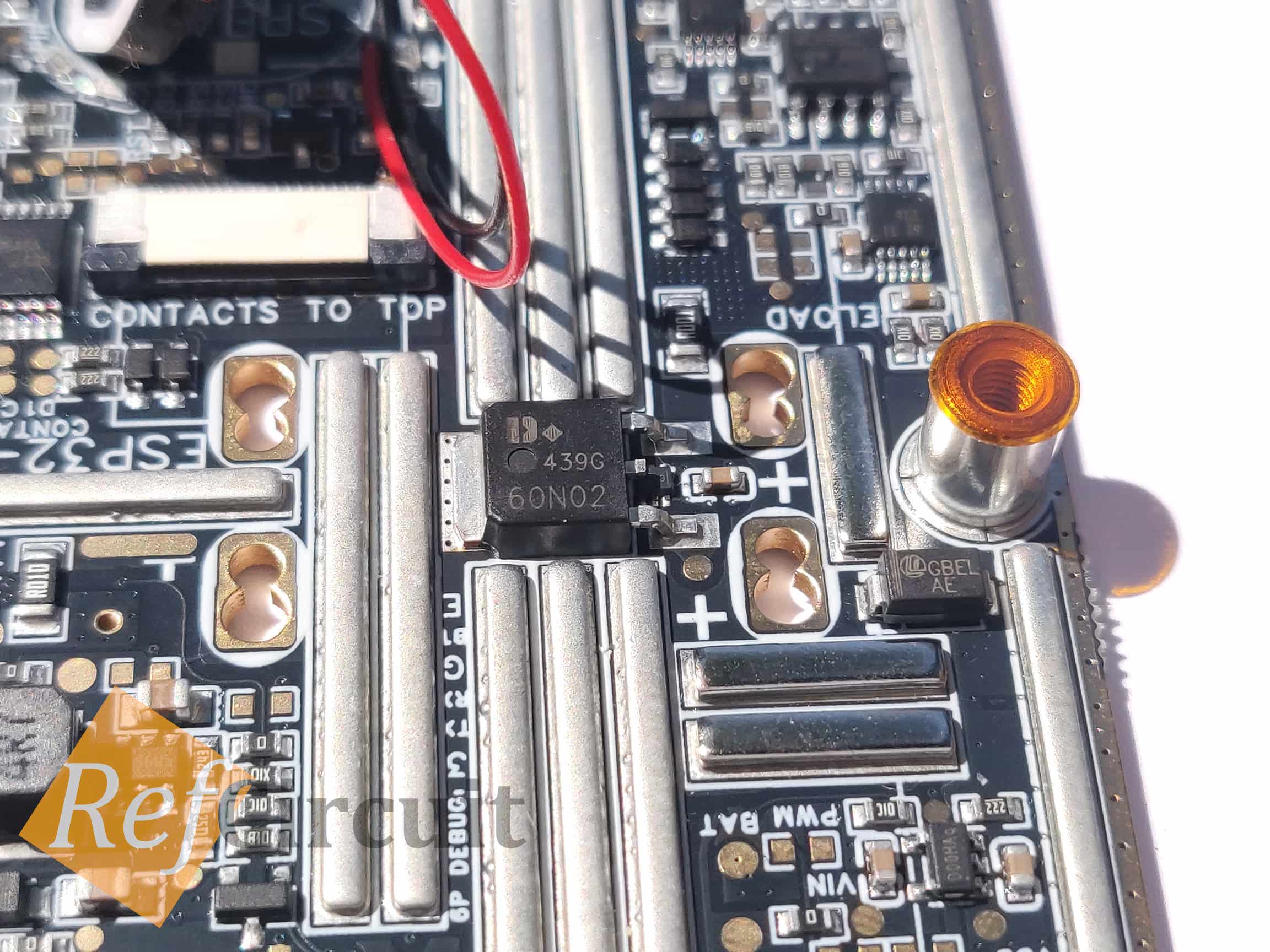
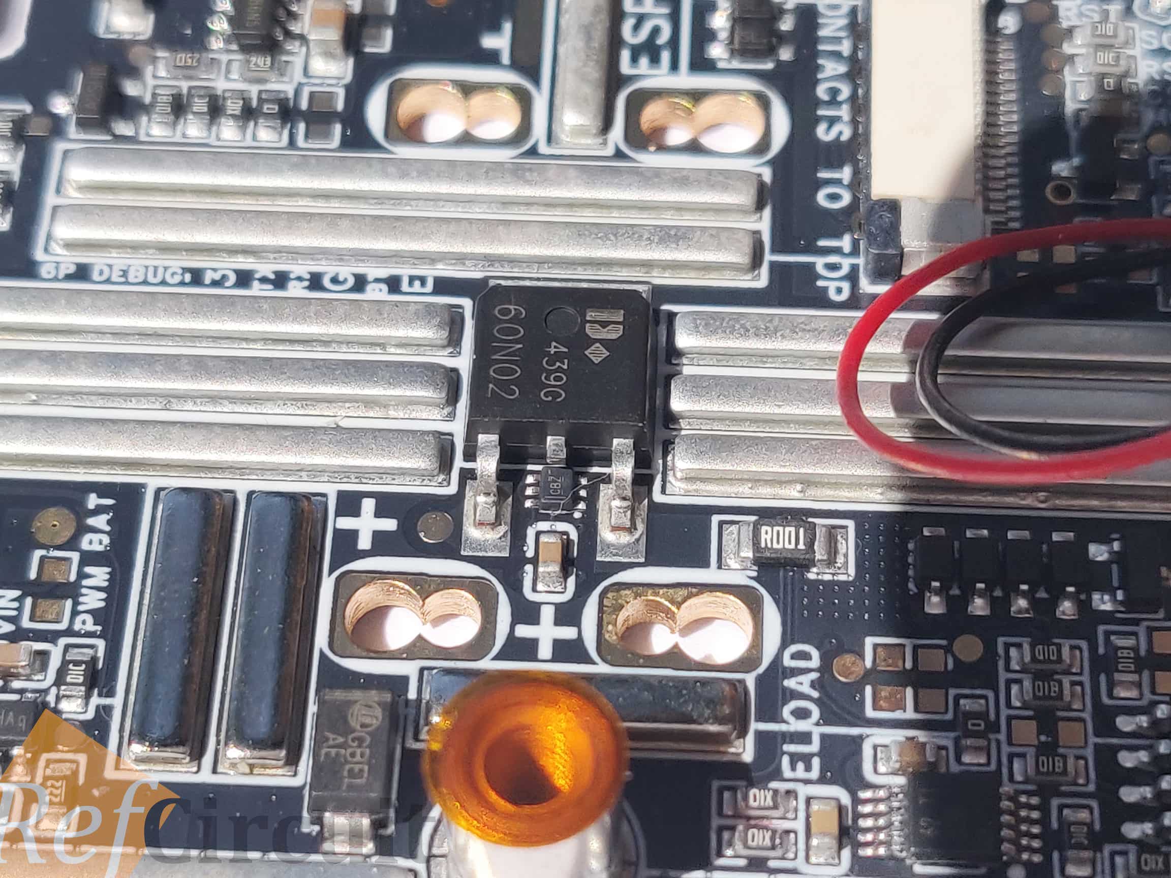
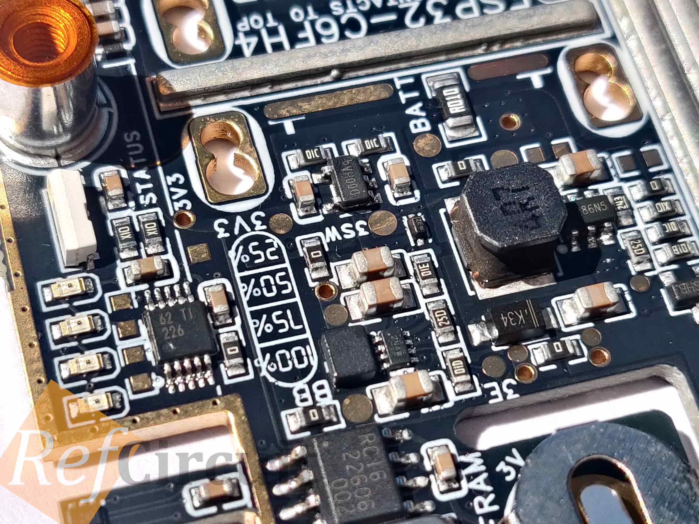
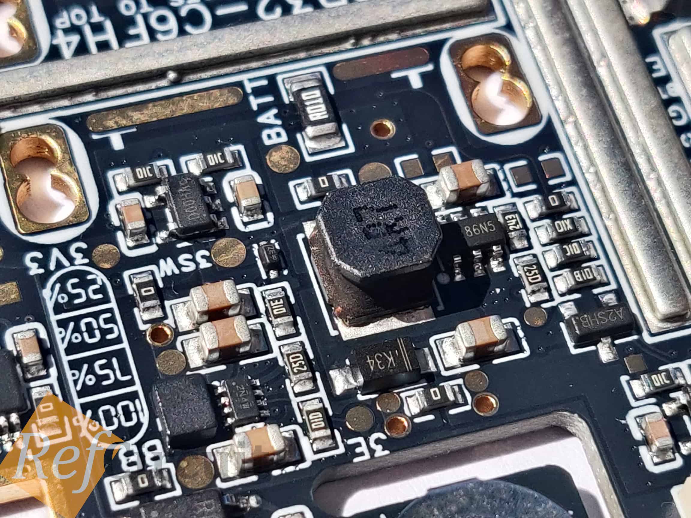
First board assembled fine, but the second board has several soldering issues:
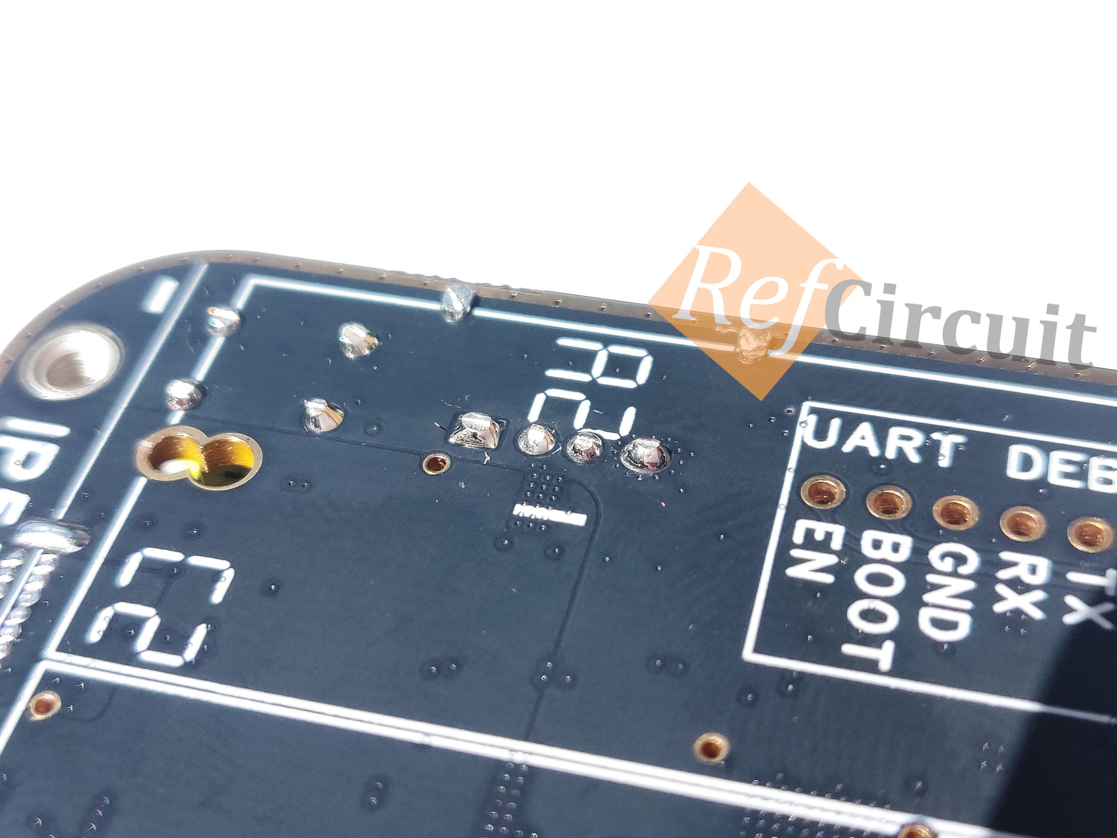
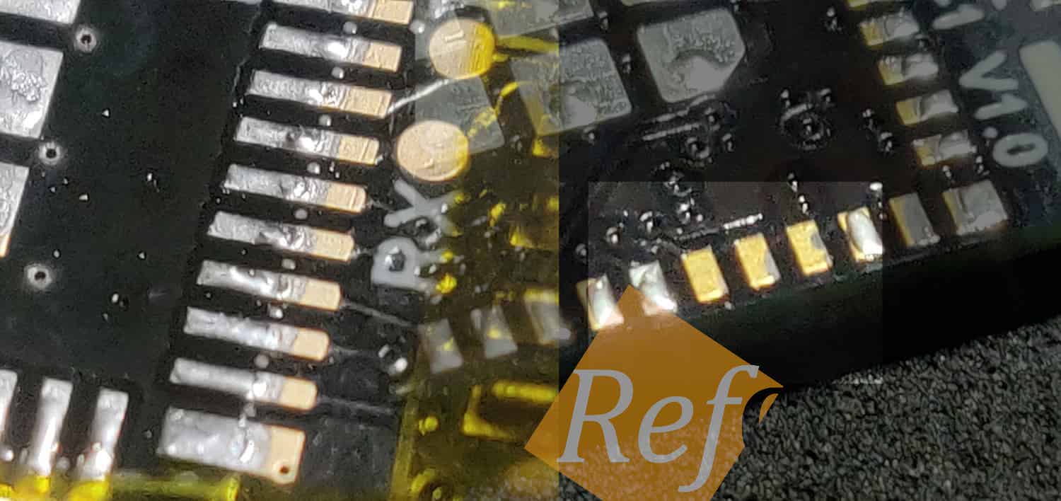
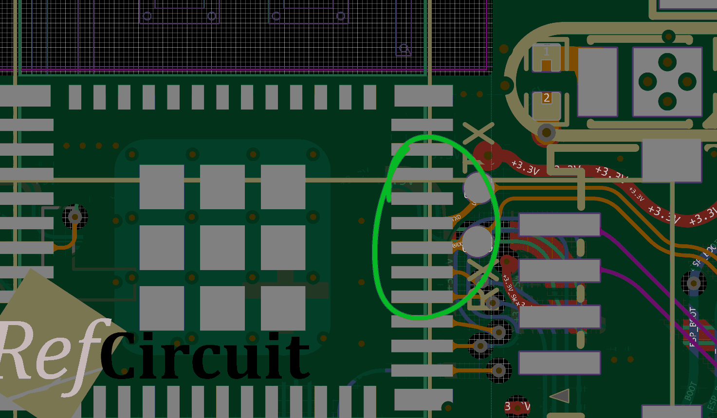
ESP Bottoms Pins
| I increased pad size for easier soldering and probing, but JLCPCB use their custom solder paste layer | |
 |  |
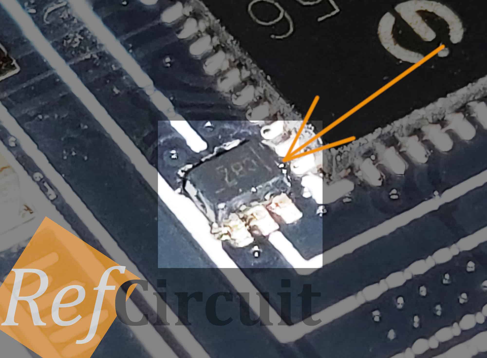
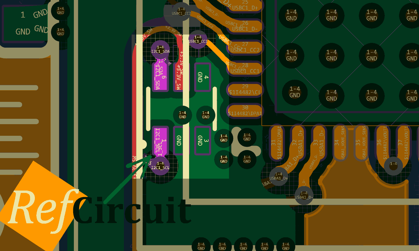
Incorrect Rotation of IC
| For any reason one of the board has incorrect IC rotation, which is manufacturing issue. As a result it was damaged and shorted +3.3V_SW rail (fortunately switch is fine because it limited current at 0.68A according to the Rset) | |
 |  |
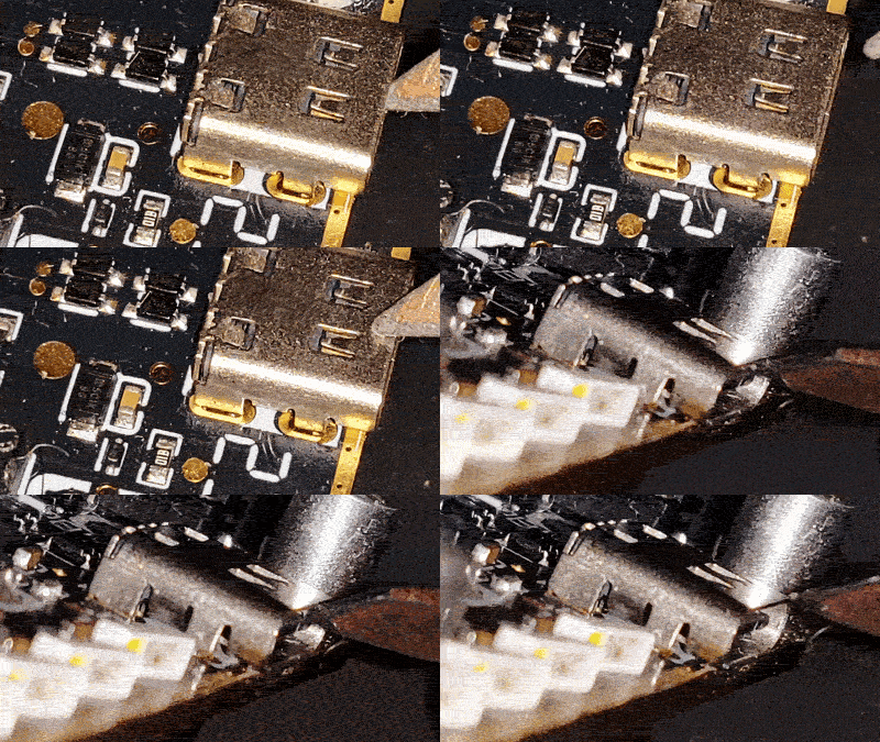
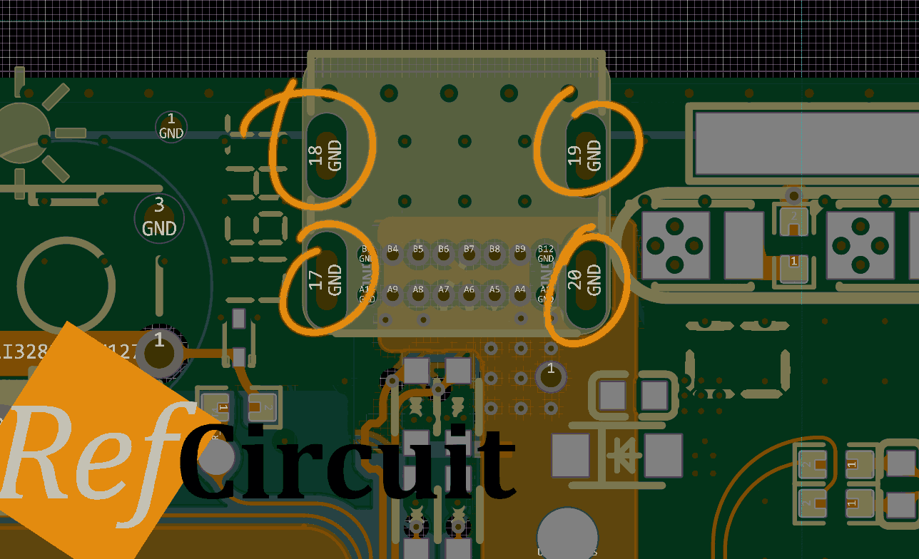
USB-C Connector
| Default footprint has THT pads without Top Solder paste. As a result one of connector has bad soldering. | |
 |  |
Conclusions
| 🟢 | Accepted 3 bare PCB and 2 assembled PCBA |
| 🟢 | Components rotation corresponds to the silkscreen marking/assembly drawing |
| 🟡 | Pins of THT components cut-offed on the bottoms side according to the remark but not perfect (~0.8mm is residual) |
| 🟡 | Leads of the NTC TS not cutted but incorrectly inserted |
| 🟡 | Top caps placed on the buttons but since diameter is less it attached using tape |
| 🟢 | Heatsink 14x14x6mm placed on the power power bank ICs |
| 🔴 | Second board has several critical issues at once |