

Experience of using JLCPCB Gold (ENIG) Edge Plating
Intro
Front pages advertise their PCB service by advanced gold edge plated boards. Let's try to use it!
Special
In theory you need to remove solder mask and clarify four unplanted places, but real manufacturer can do it without problems and I recommend this variant.
Gerber Files
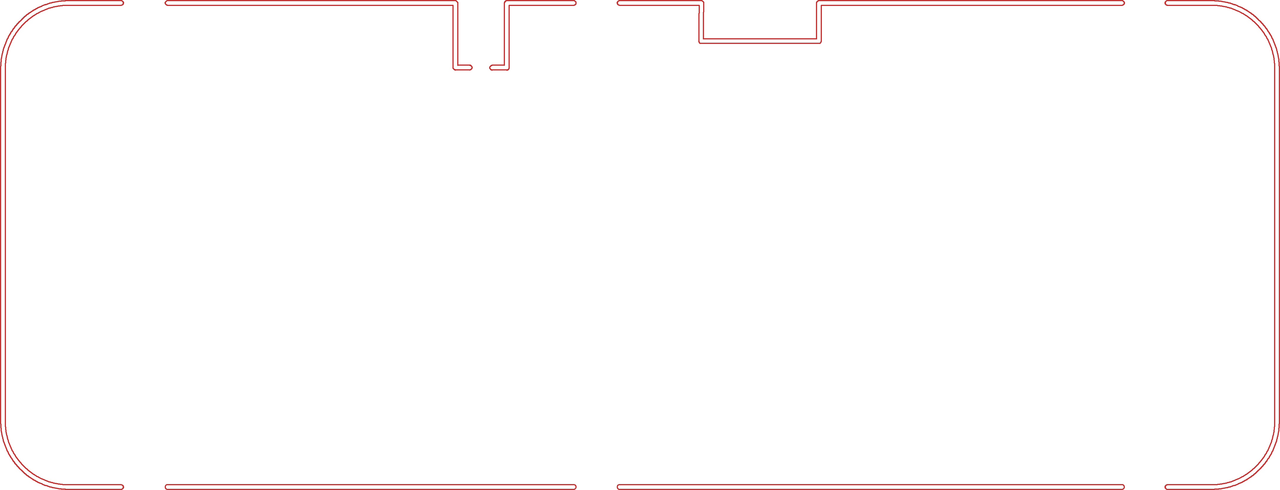
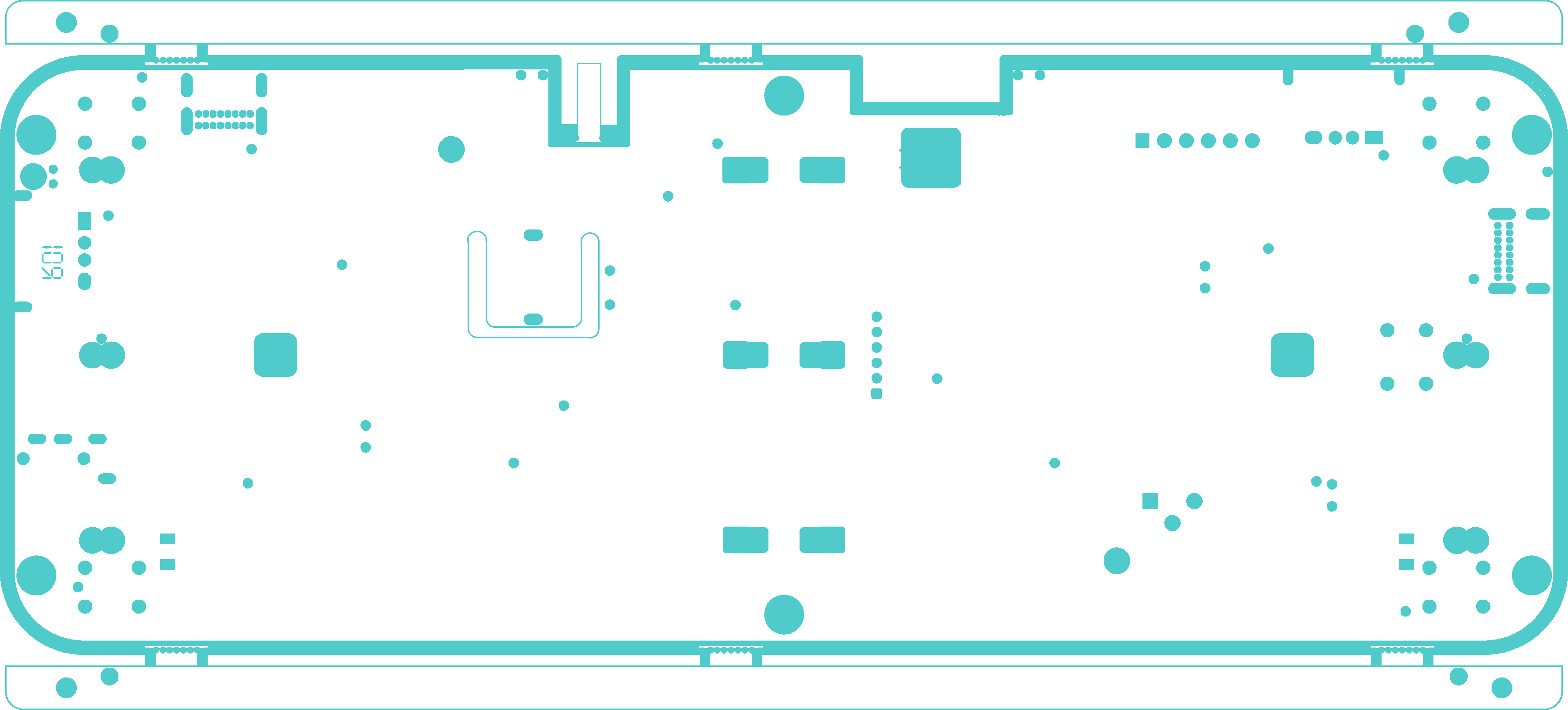
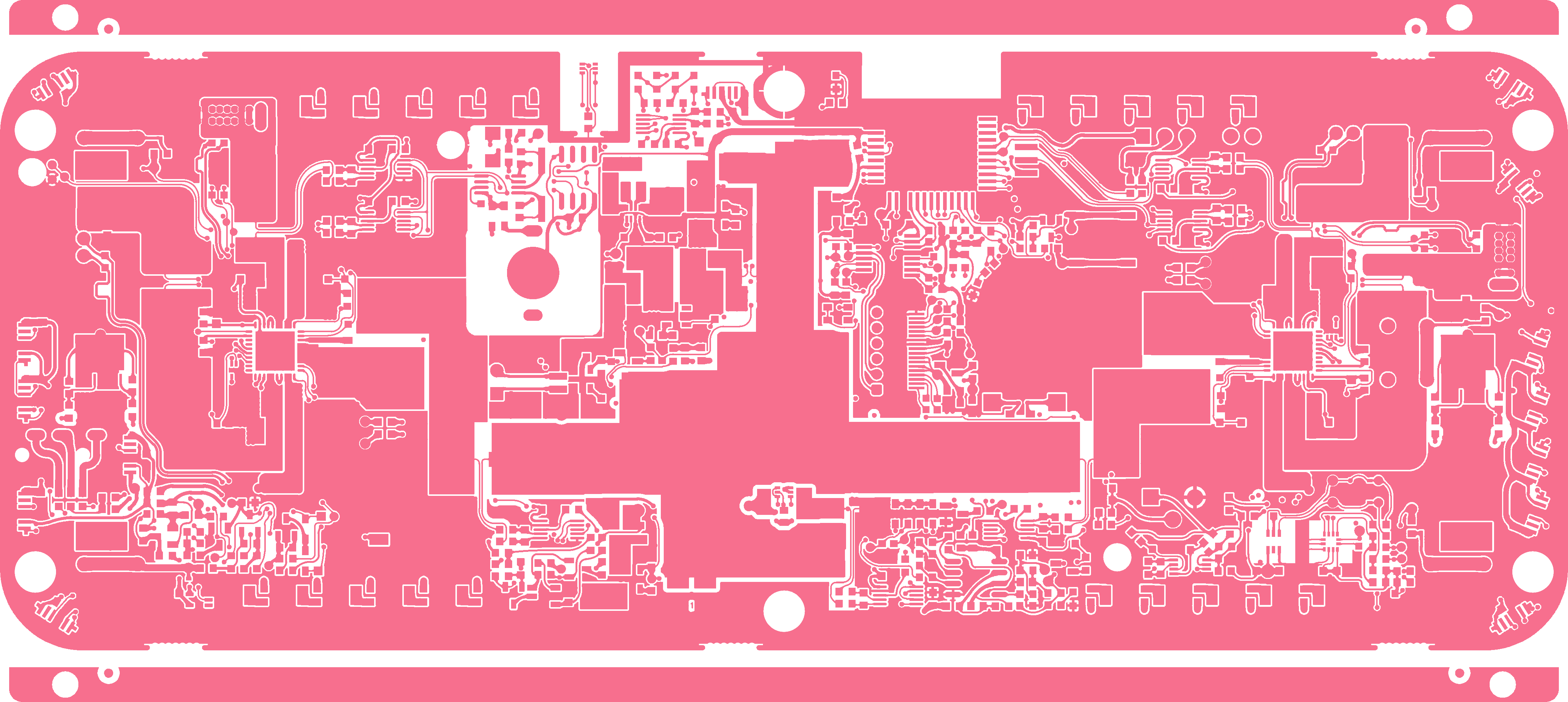
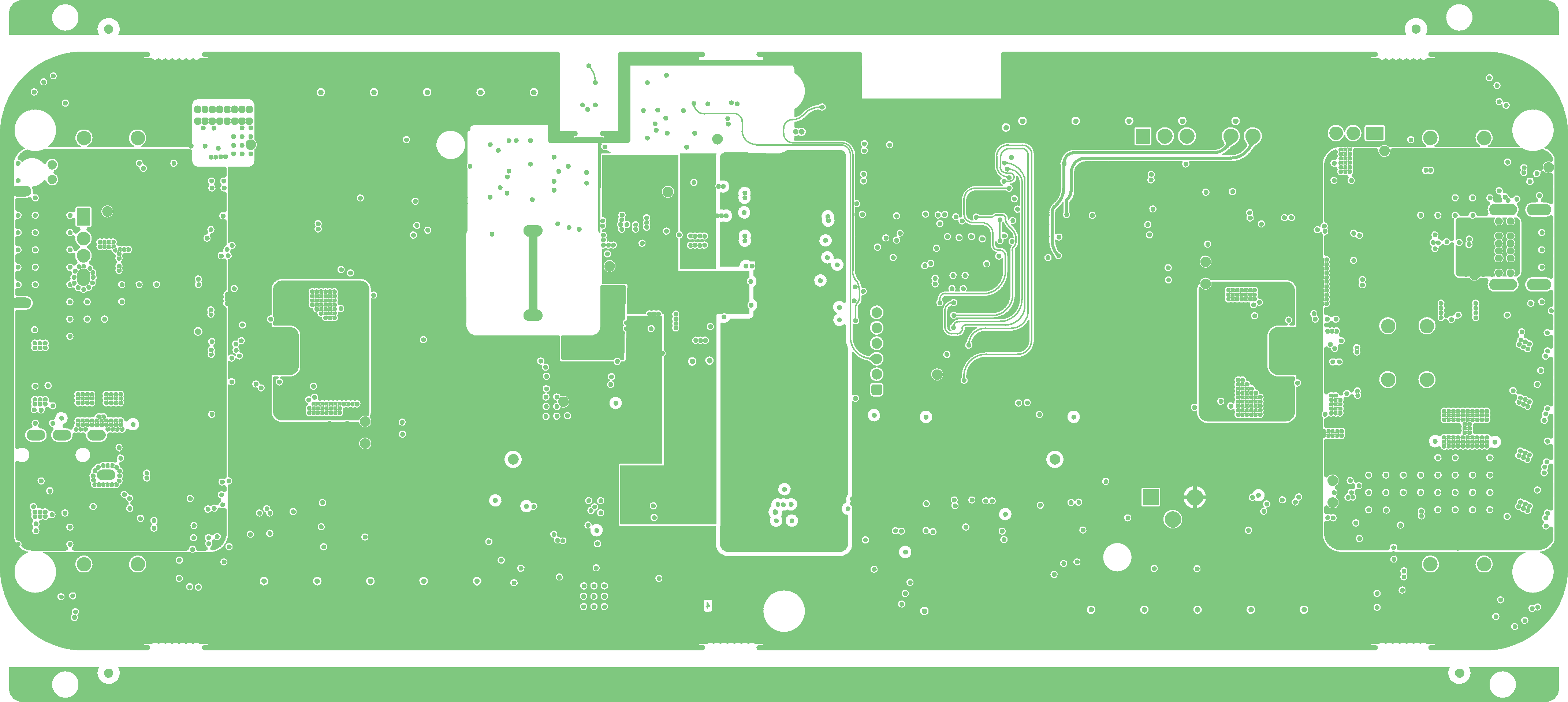
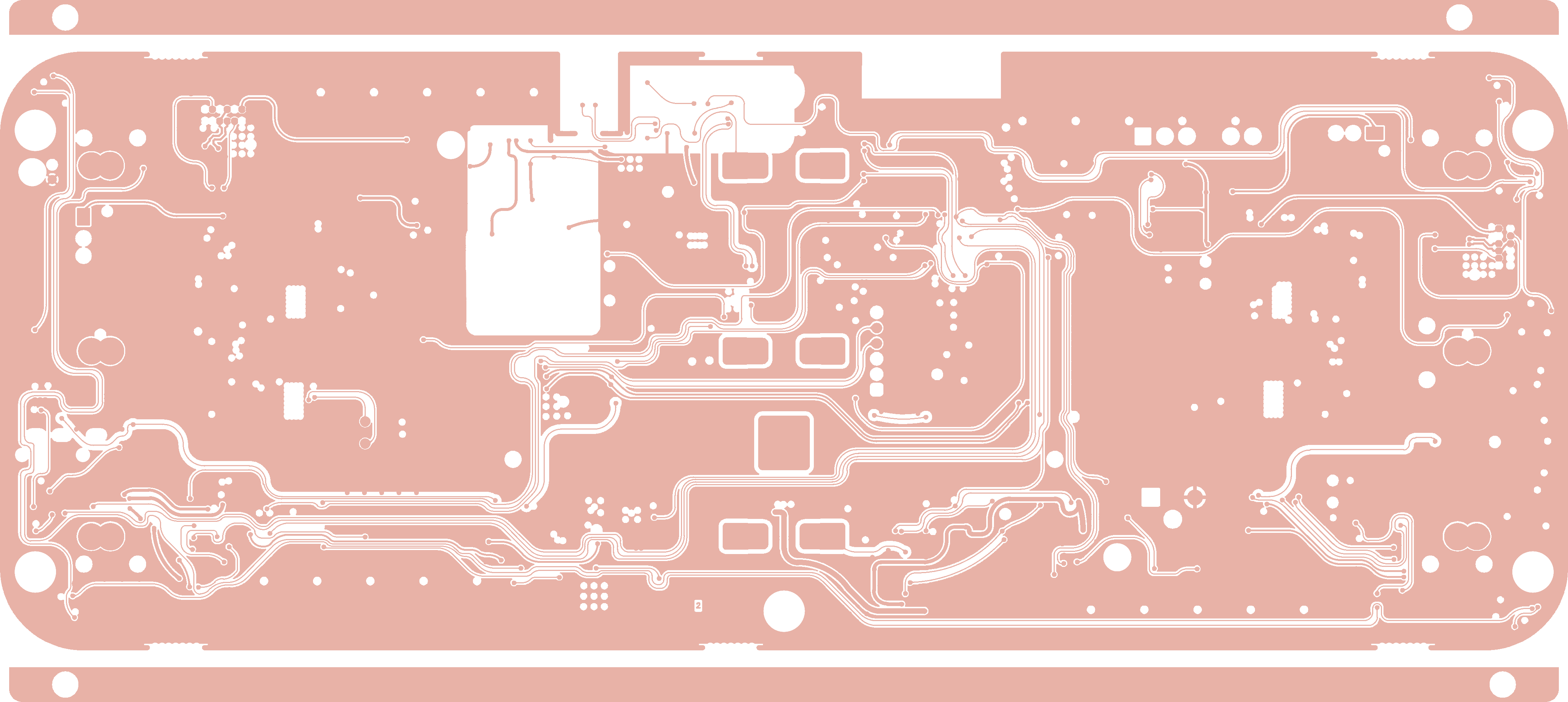
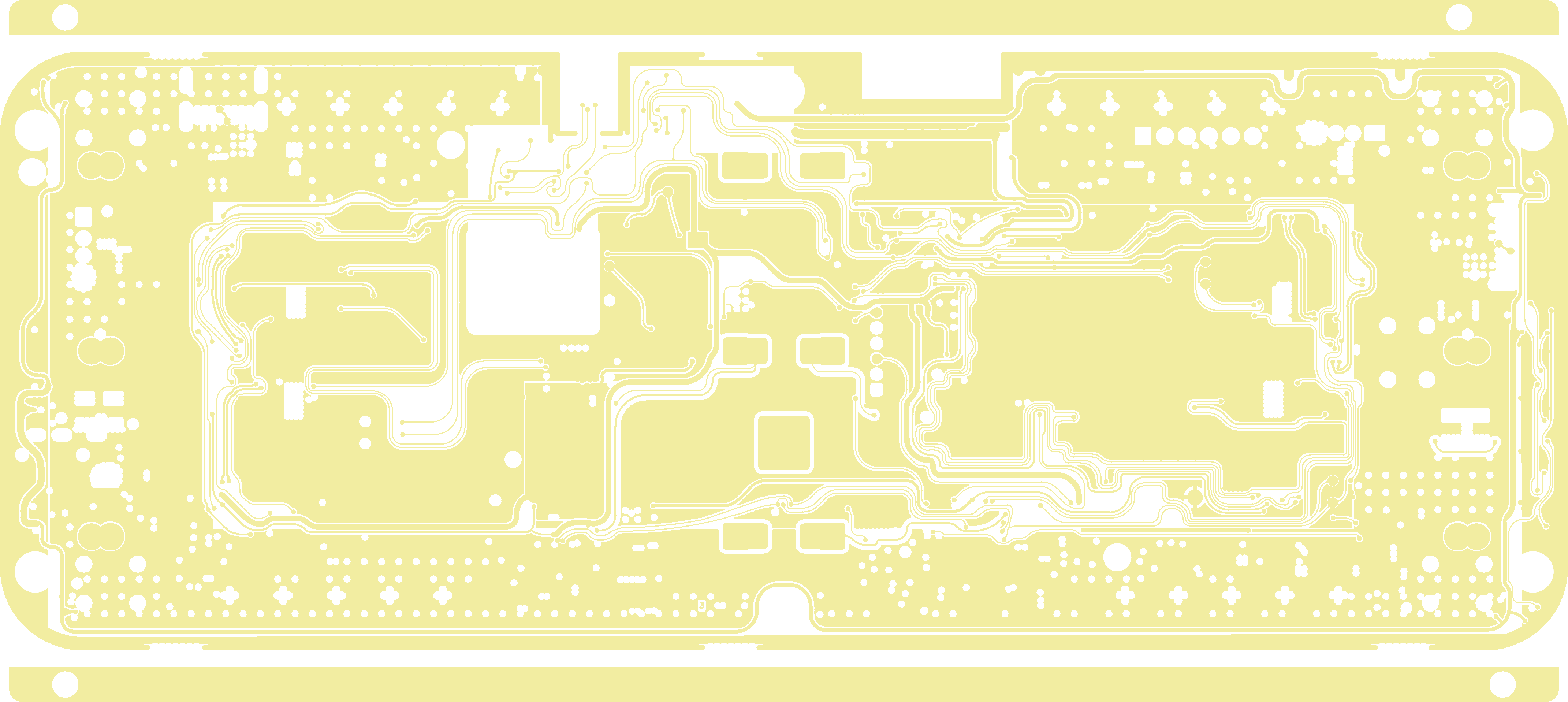
It has additional layer called baobian, which defines edge plating.
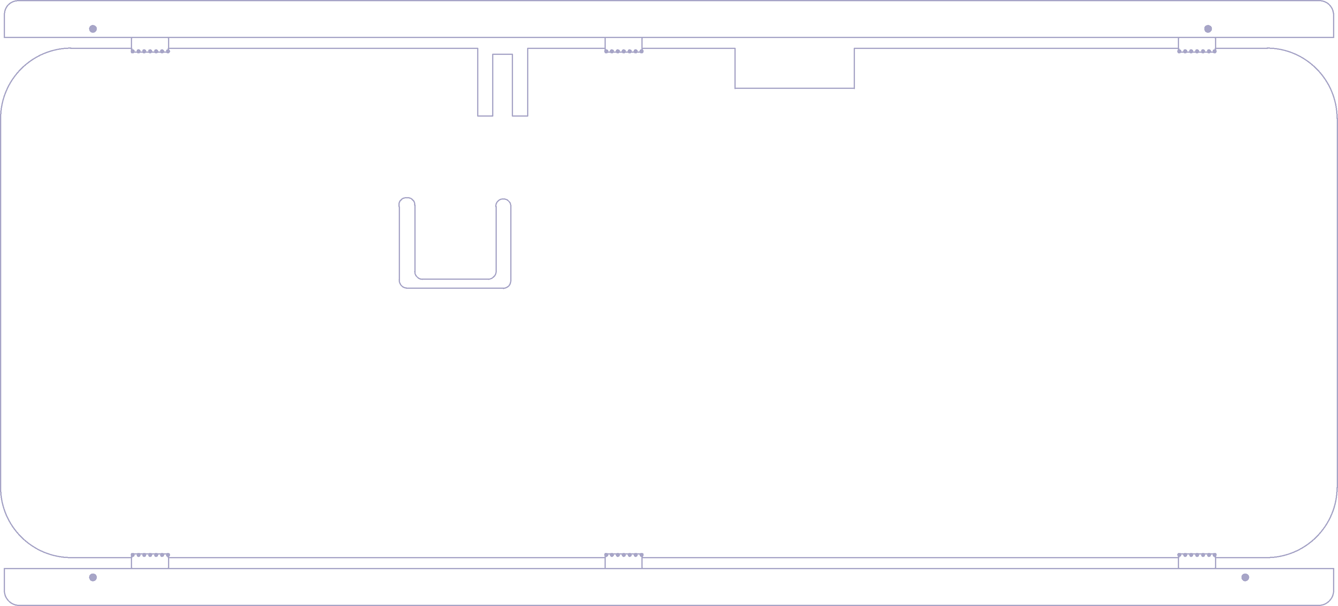
The JLC can't made plating across all perimeter and need some holes:
| baobian | |
 | |
| ko | ko1 |
 |  |
| drl | sk |
 | 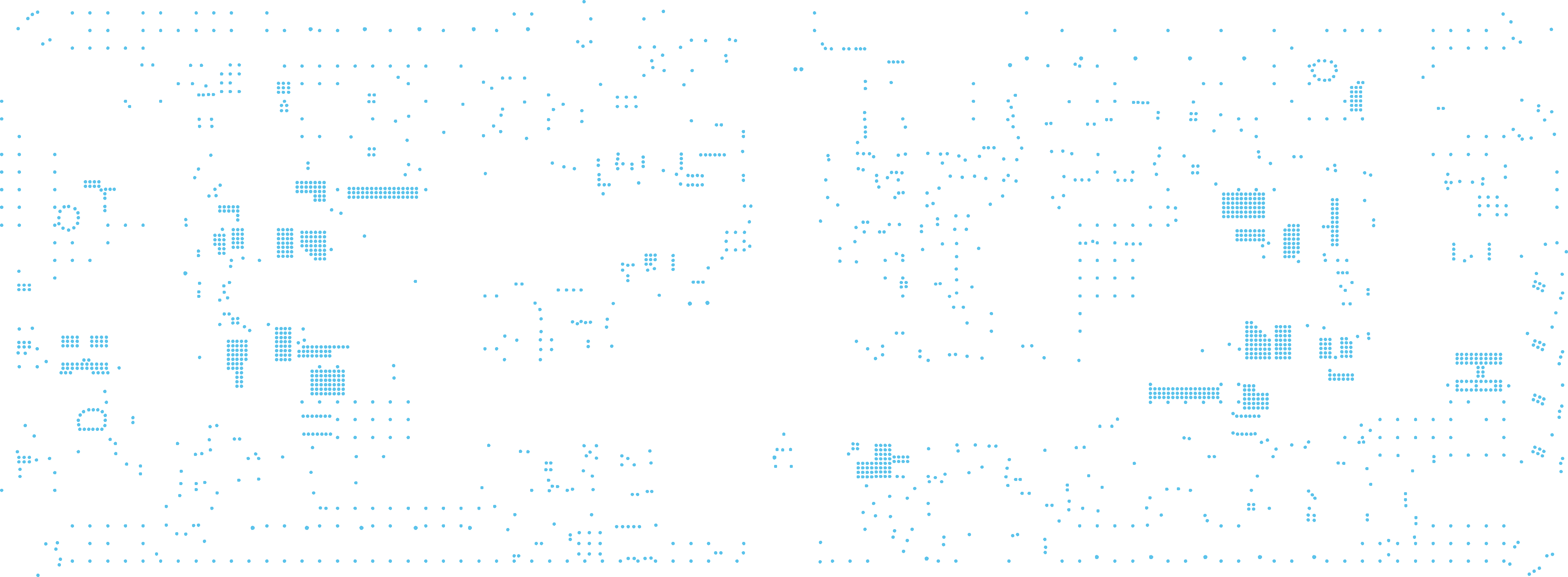 |
| to | bo |
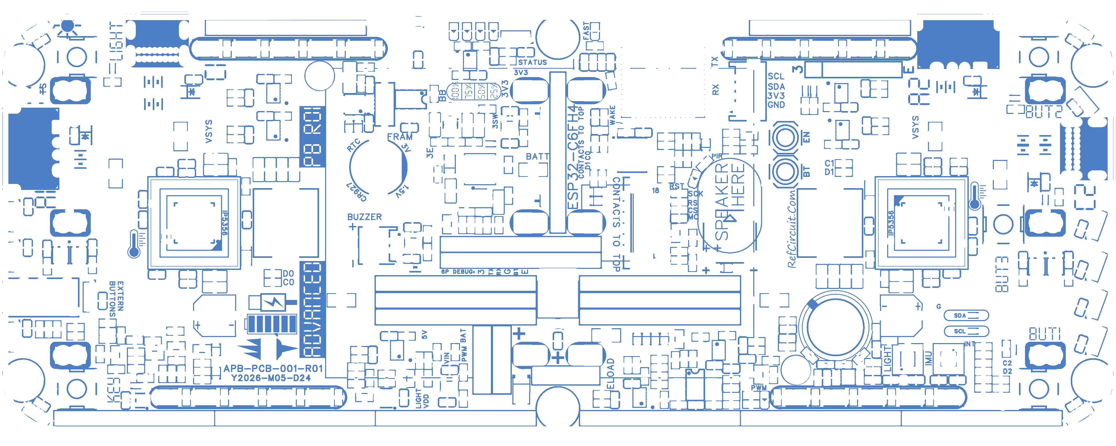 | 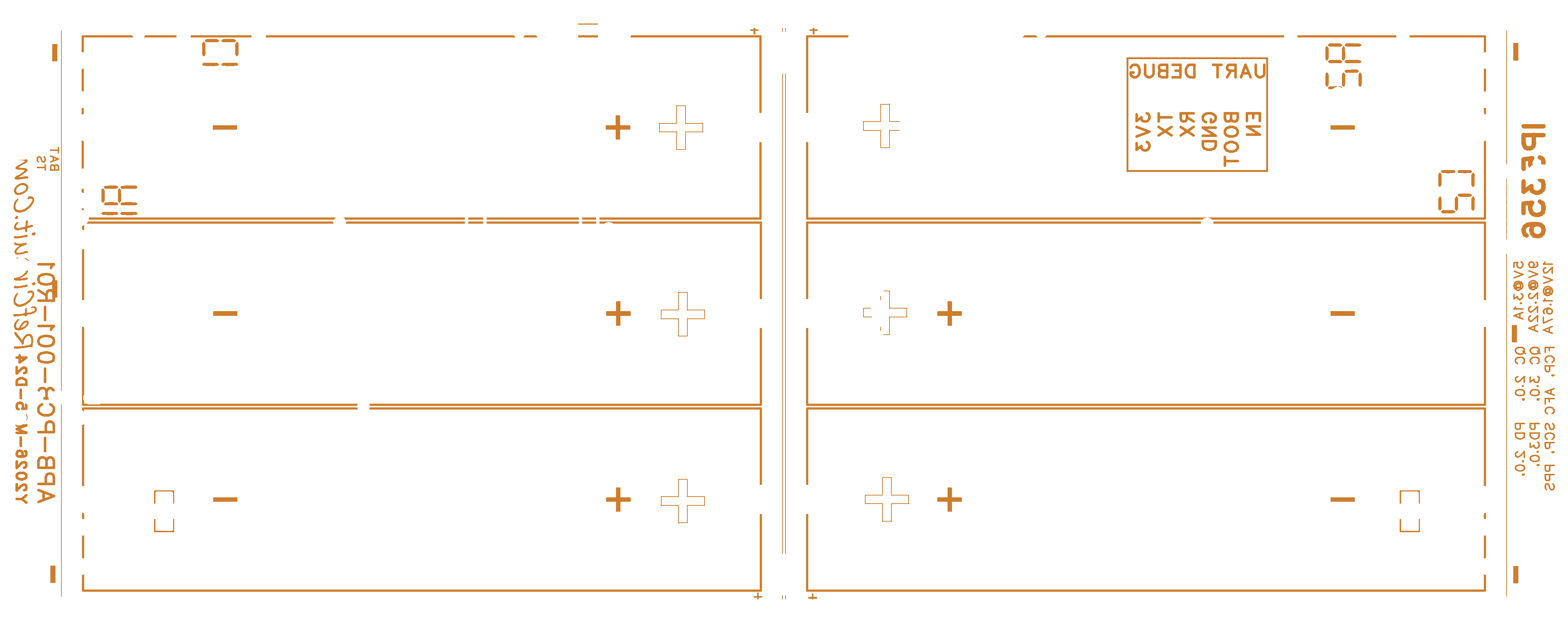 |
| ts | bs |
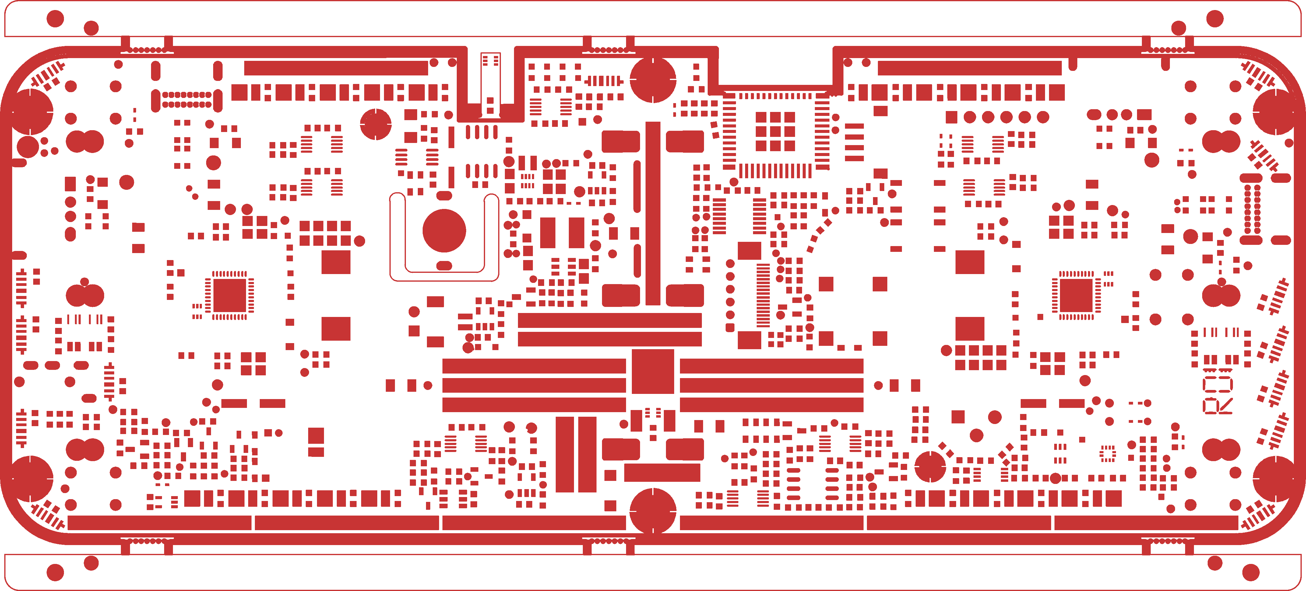 |  |
| tl | bl |
 |  |
| l2 | l3 |
 |  |
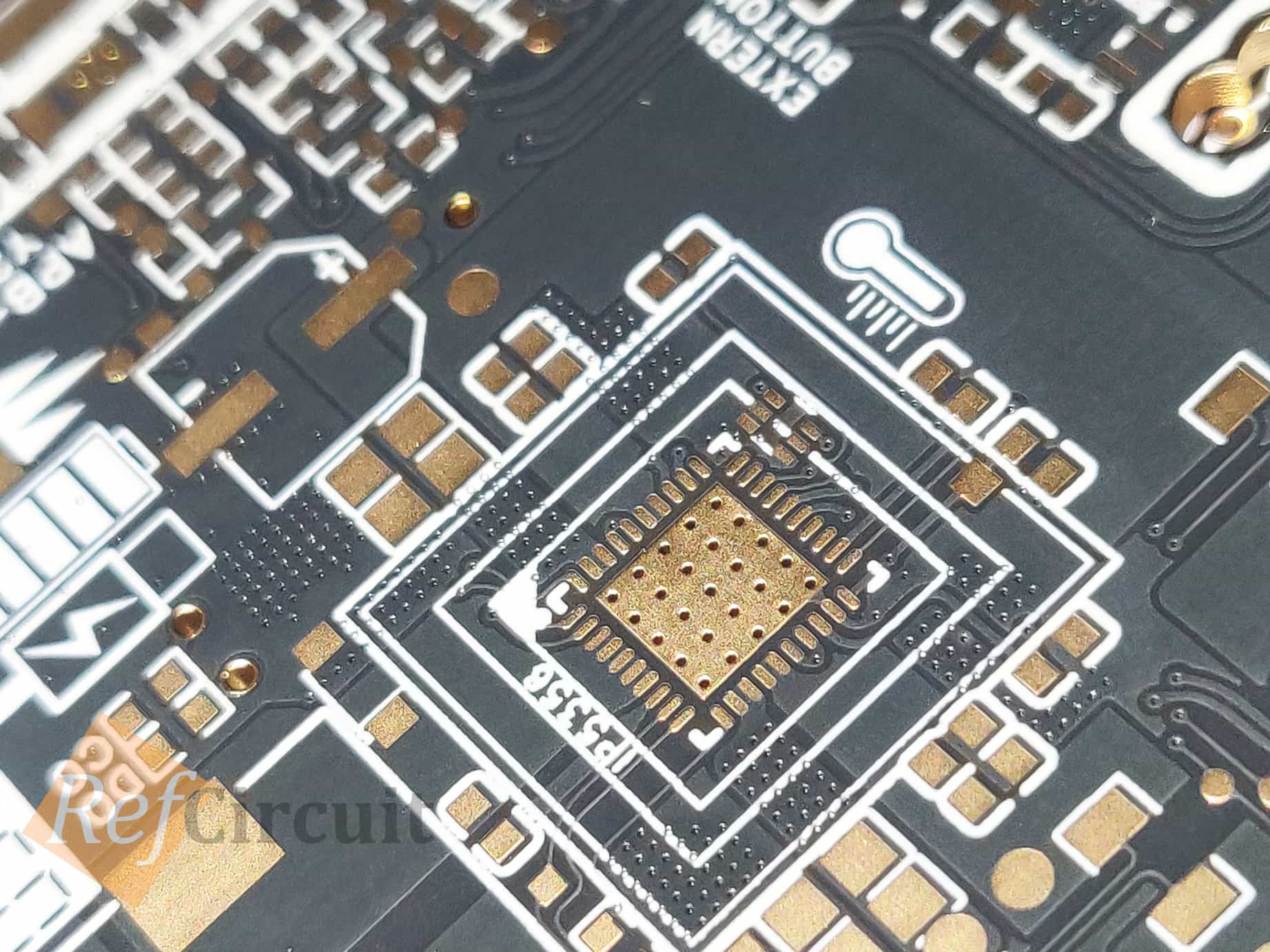
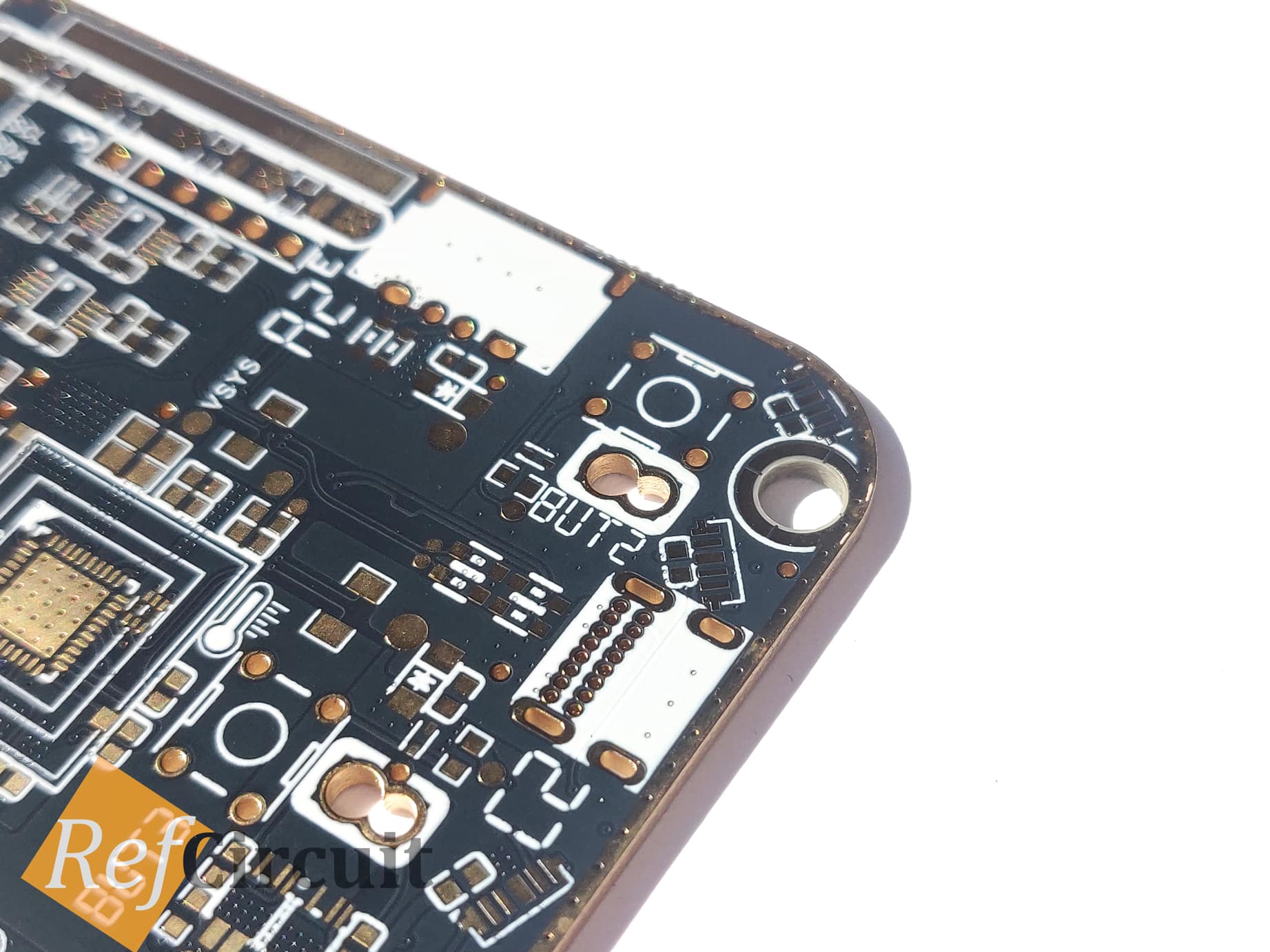
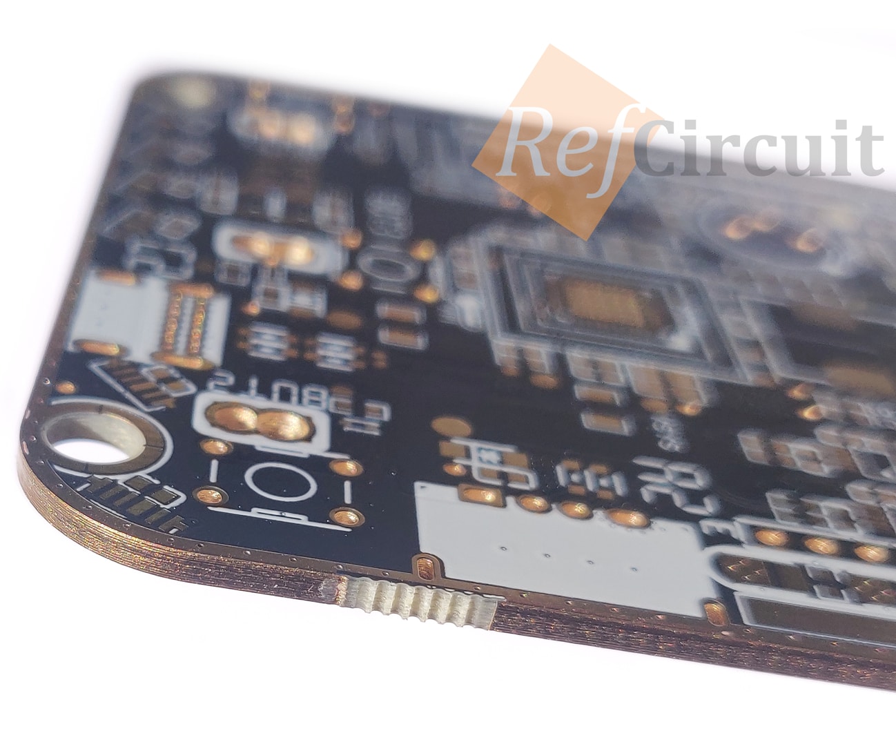
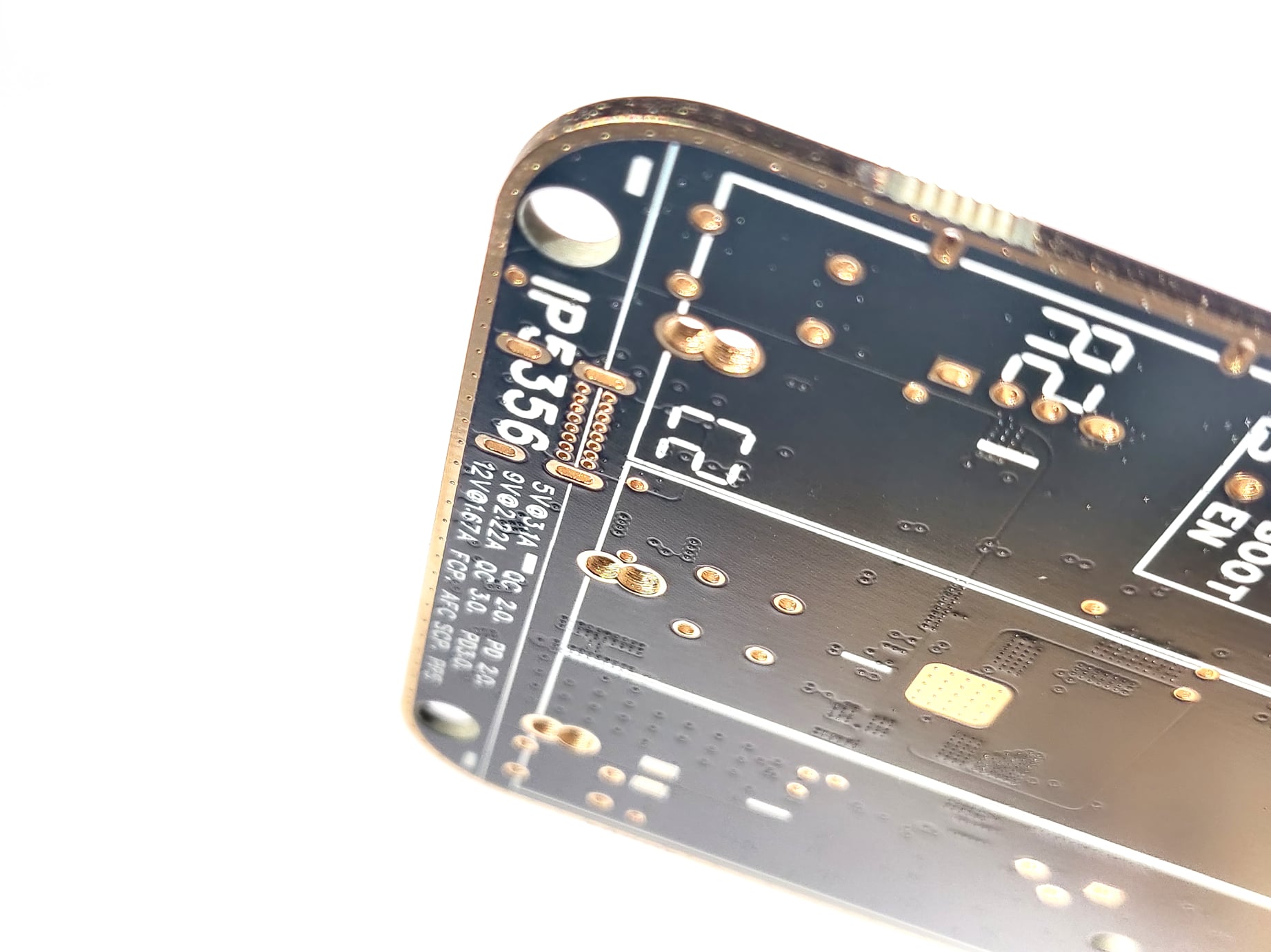
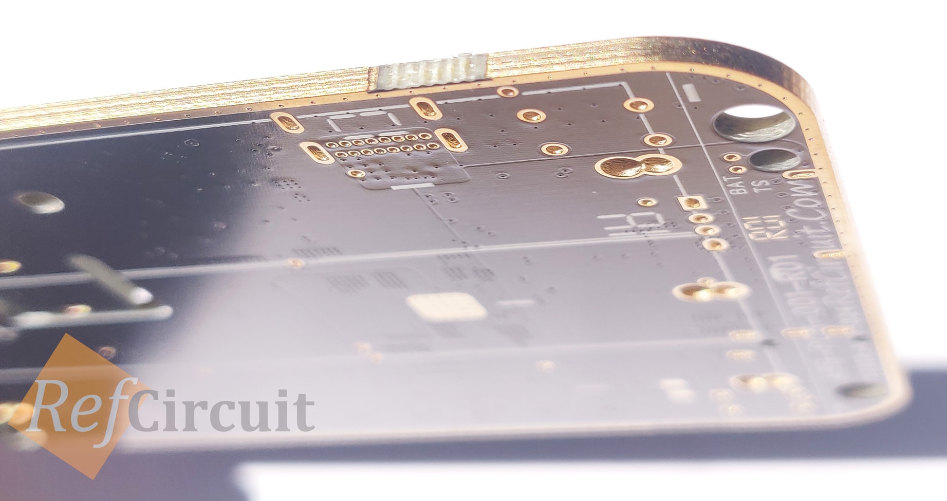
Final Results
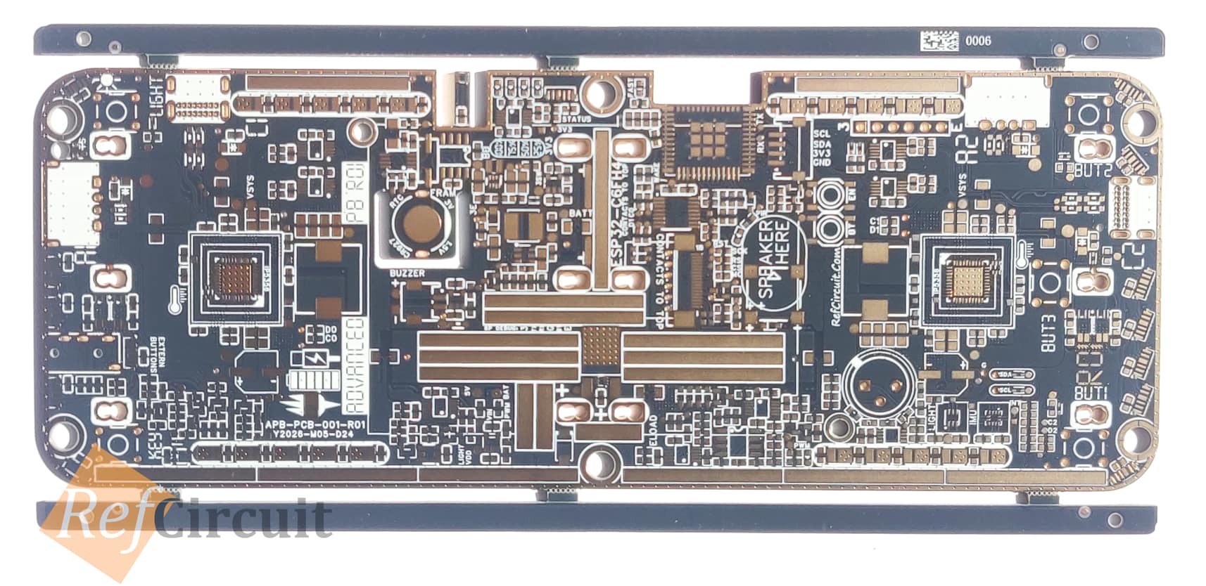
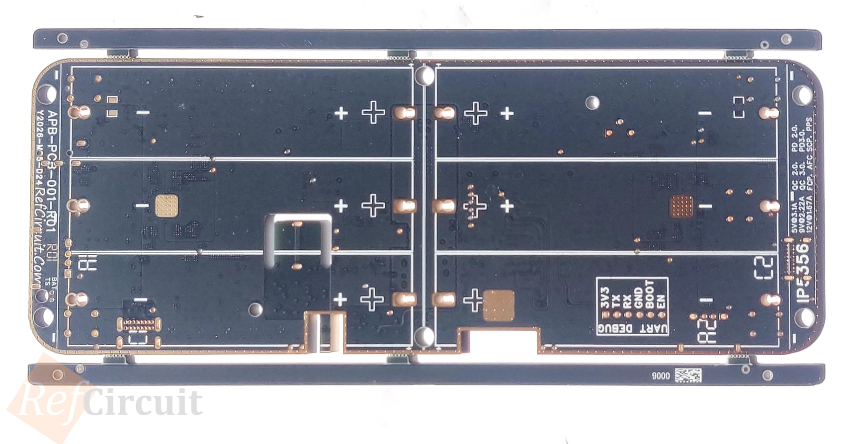
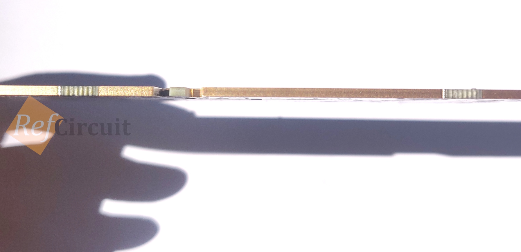
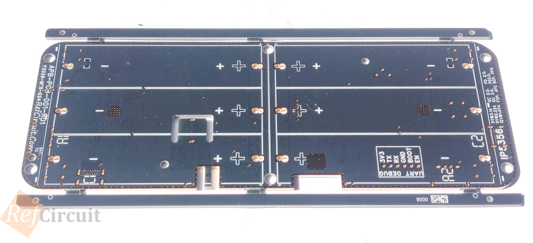
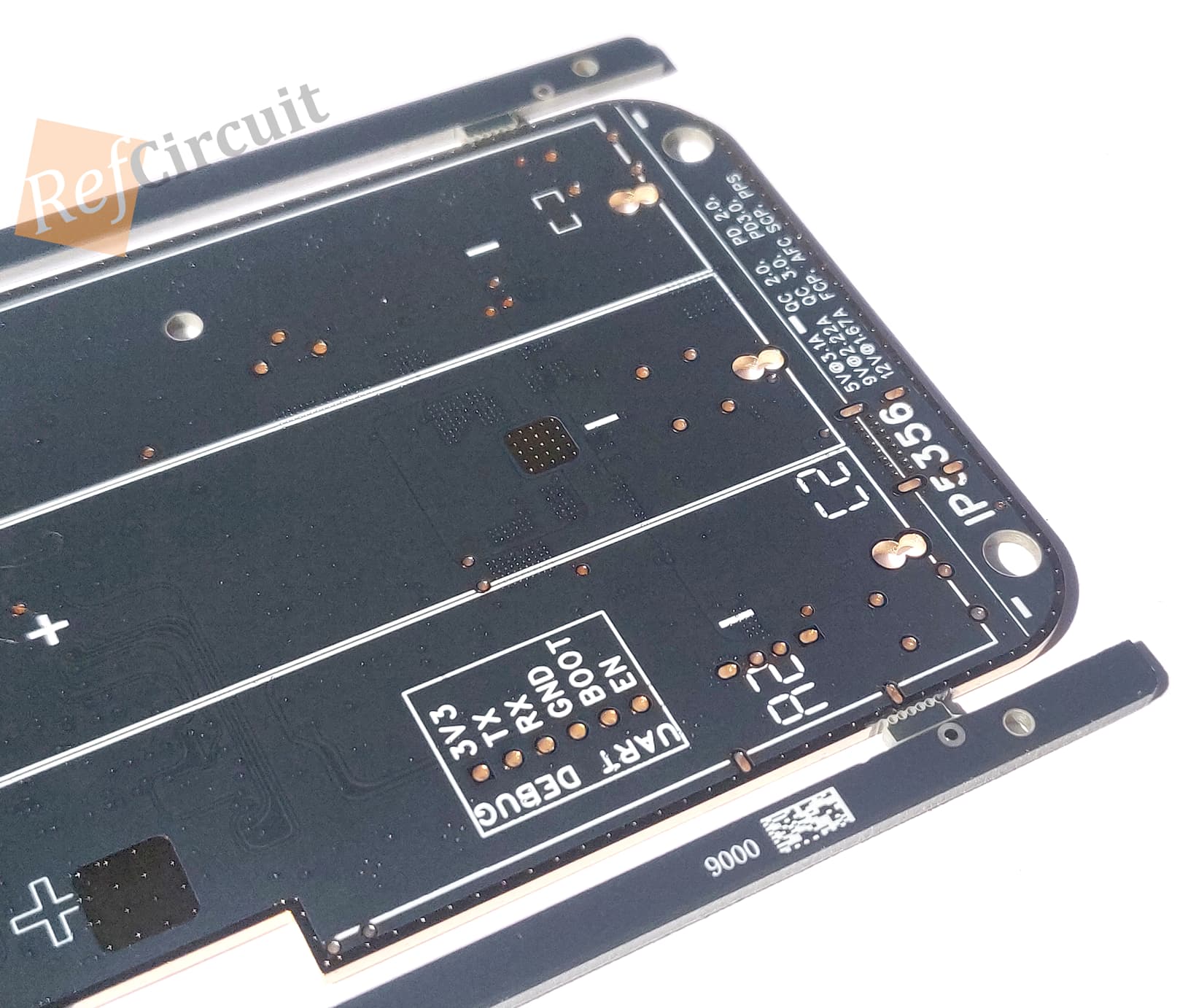
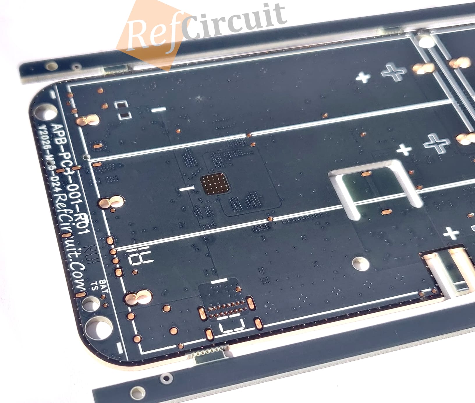
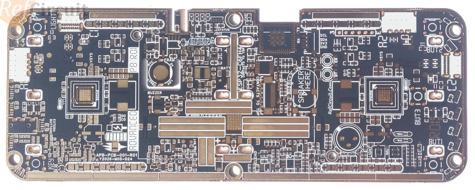
The edges are pleasant to the touch, but not looks super solid.
 |  |
 |  |
 |  |
 | 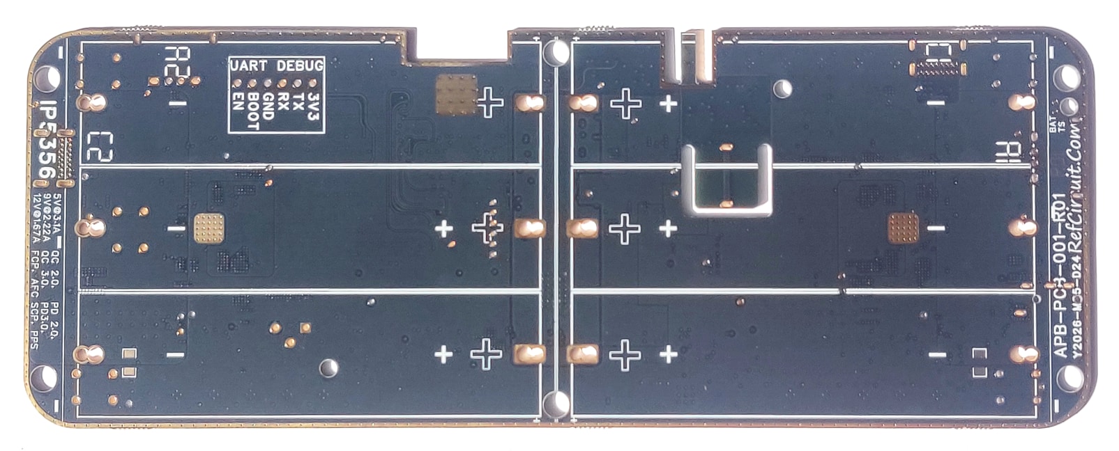 |
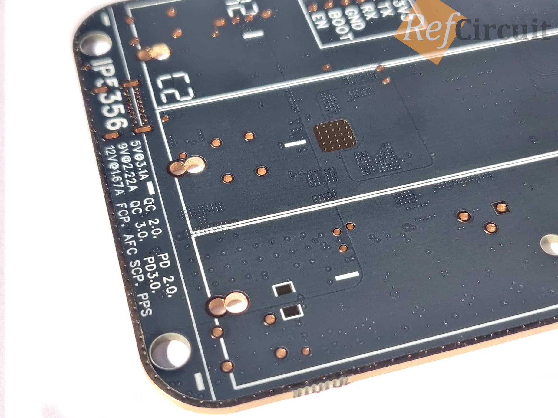 | 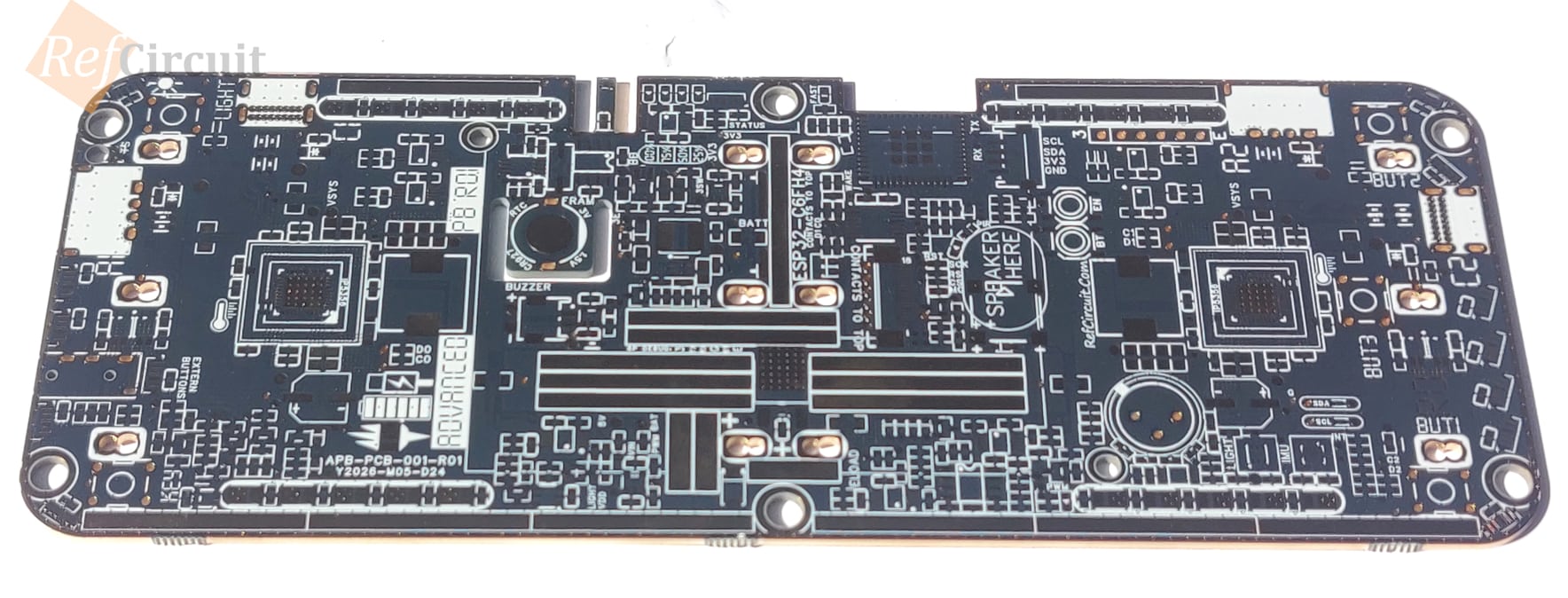 |
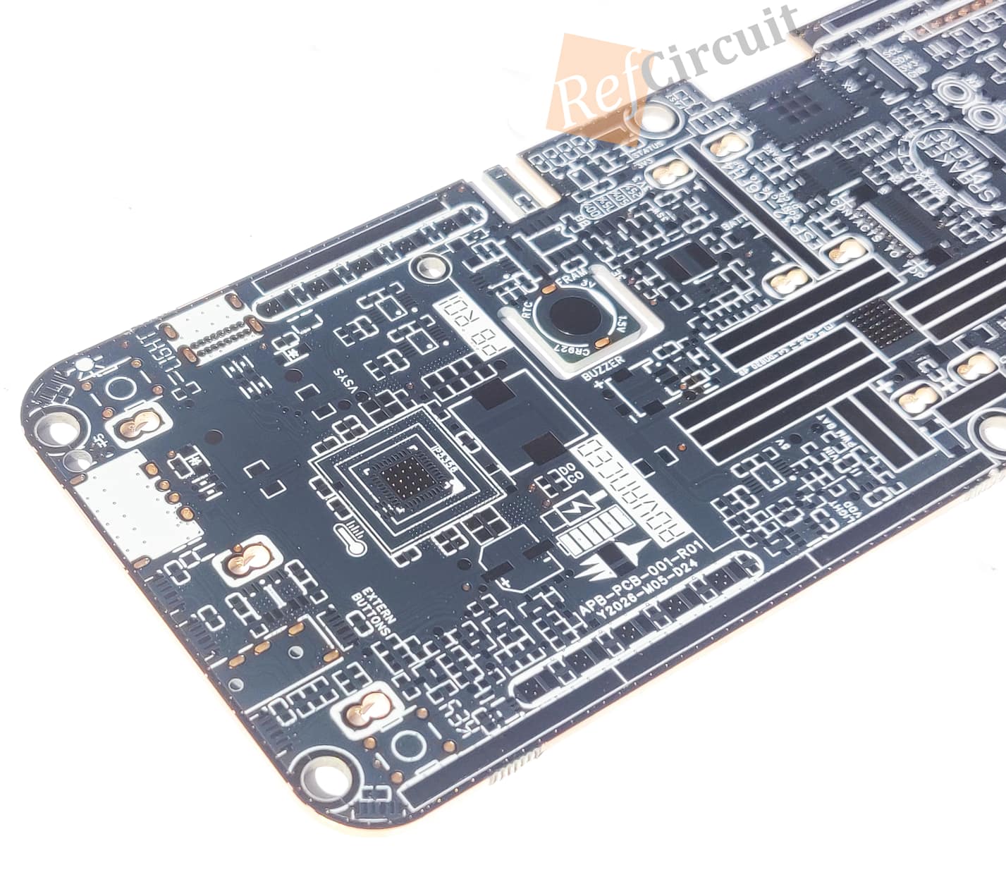 | 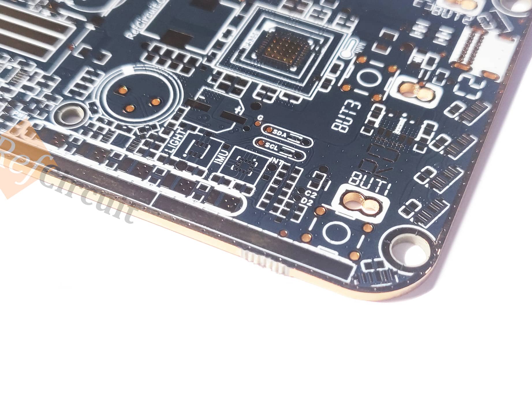 |
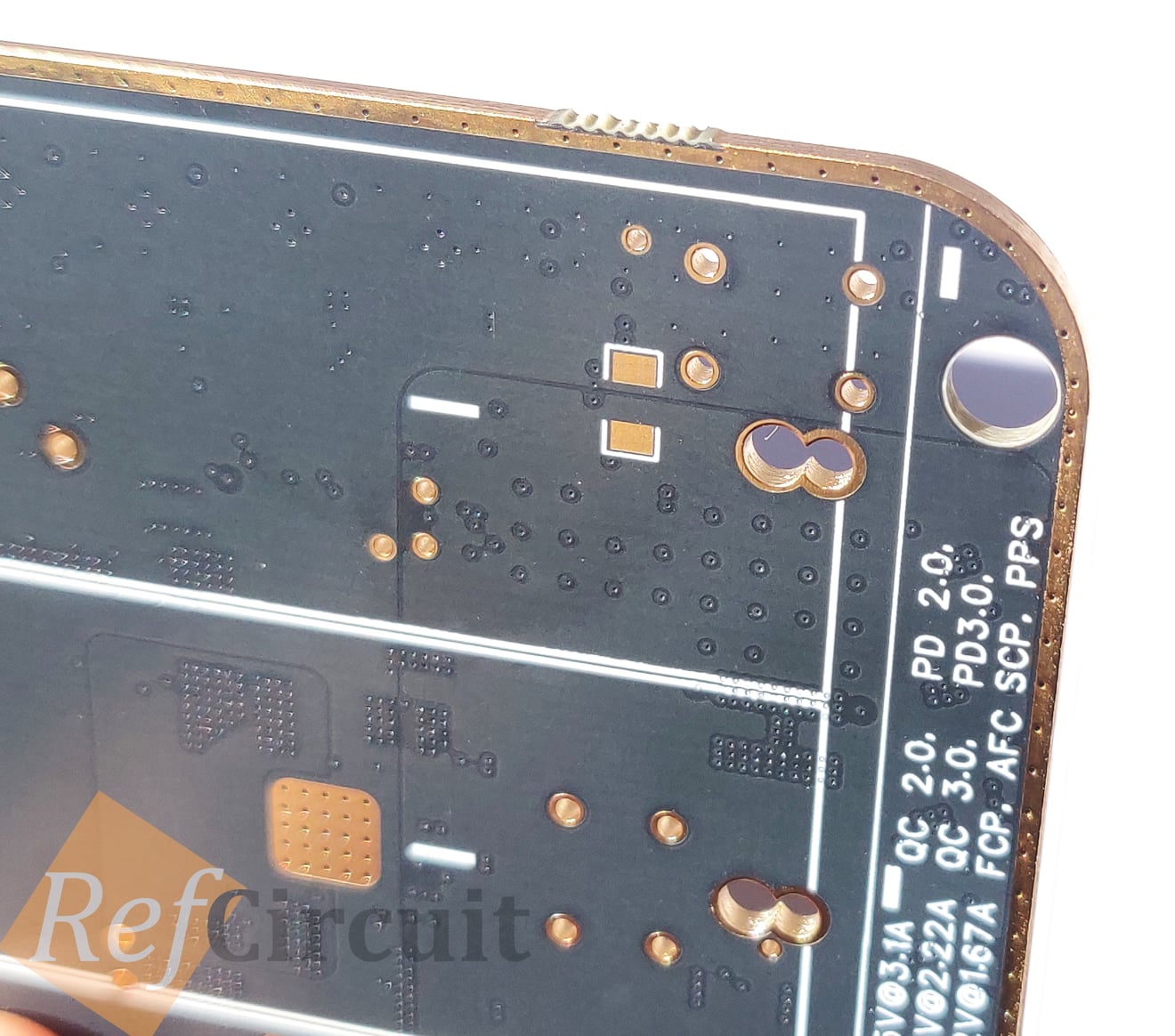 | 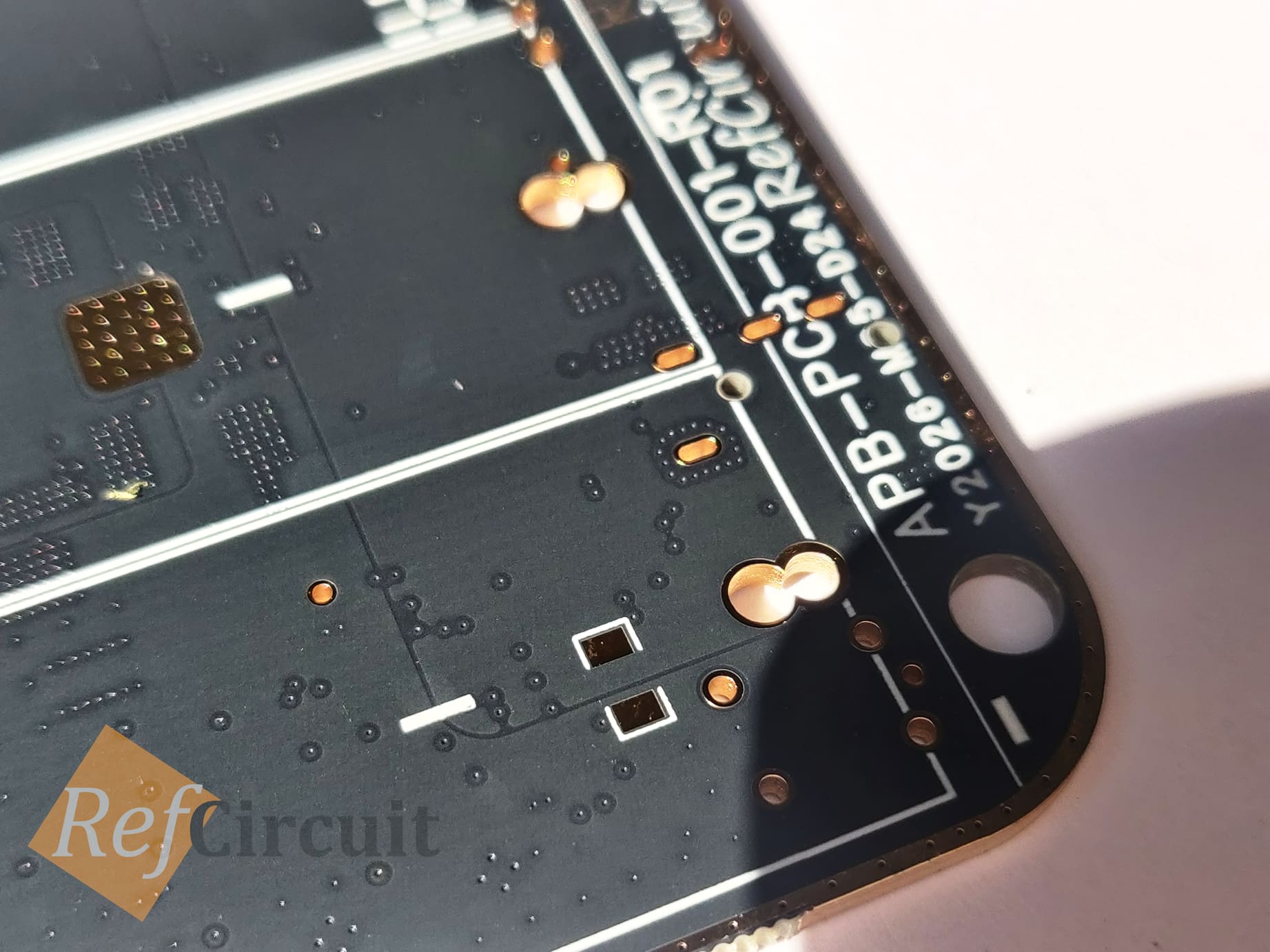 |
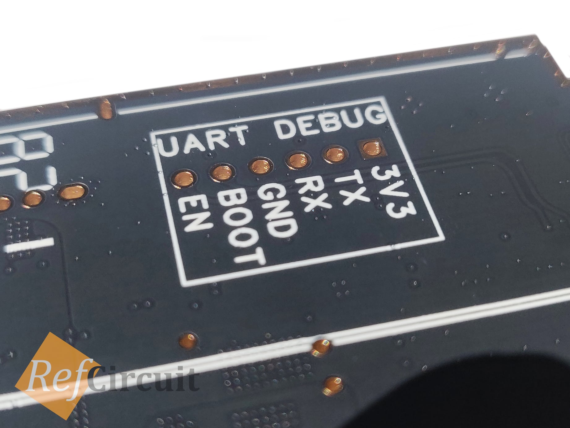 | 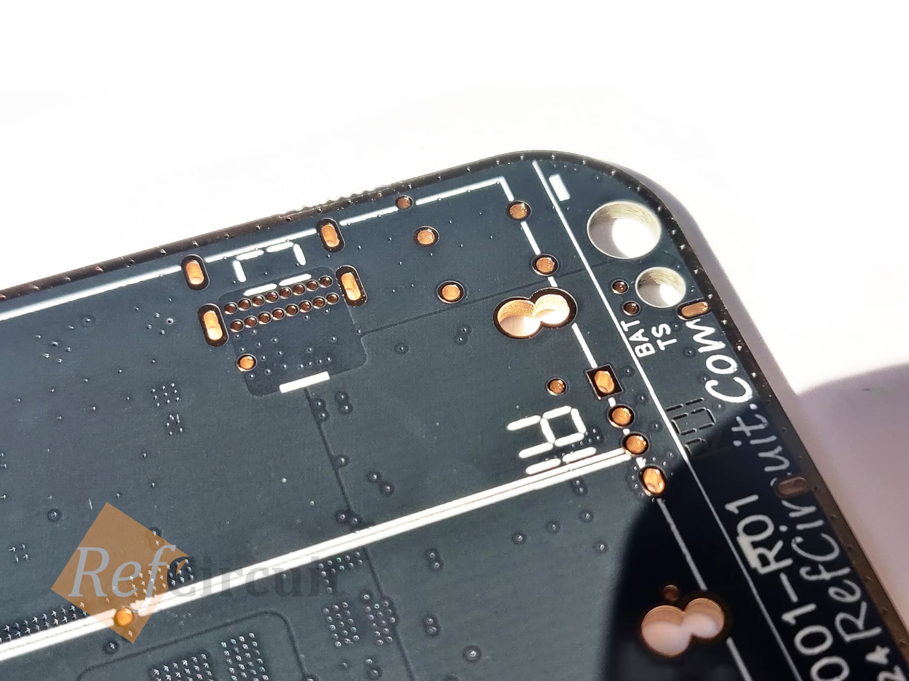 |
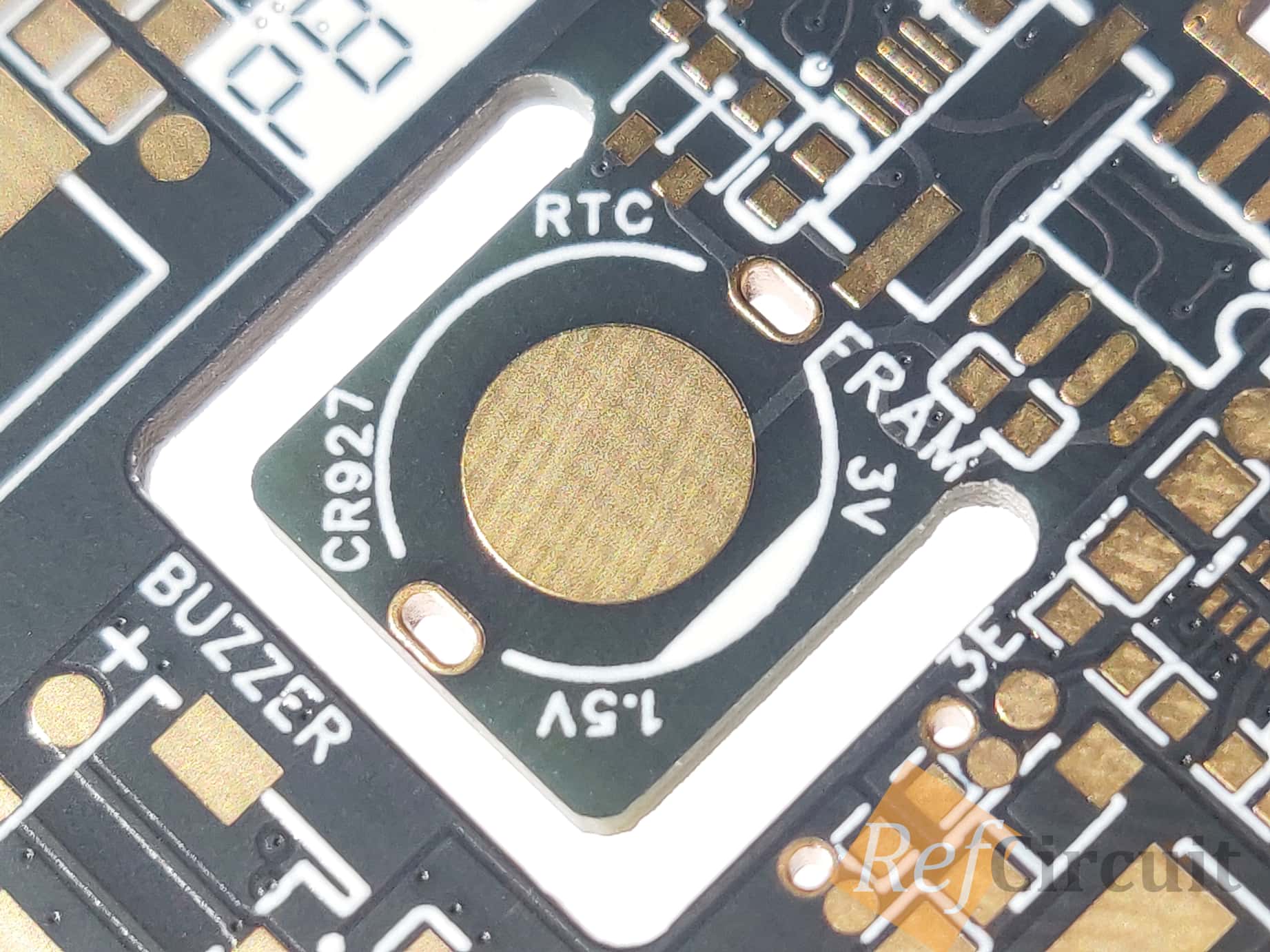 | 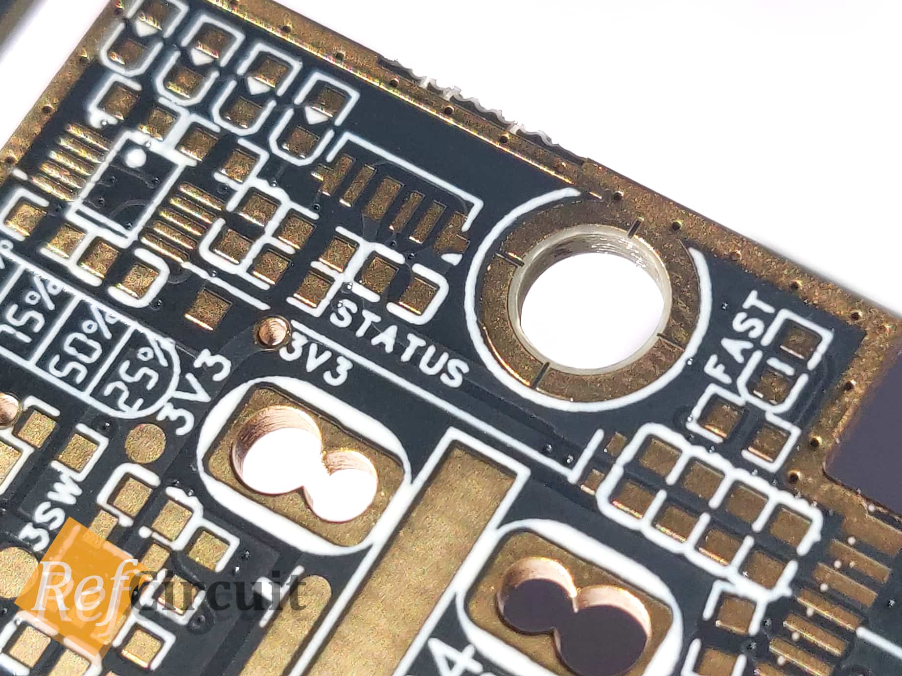 |
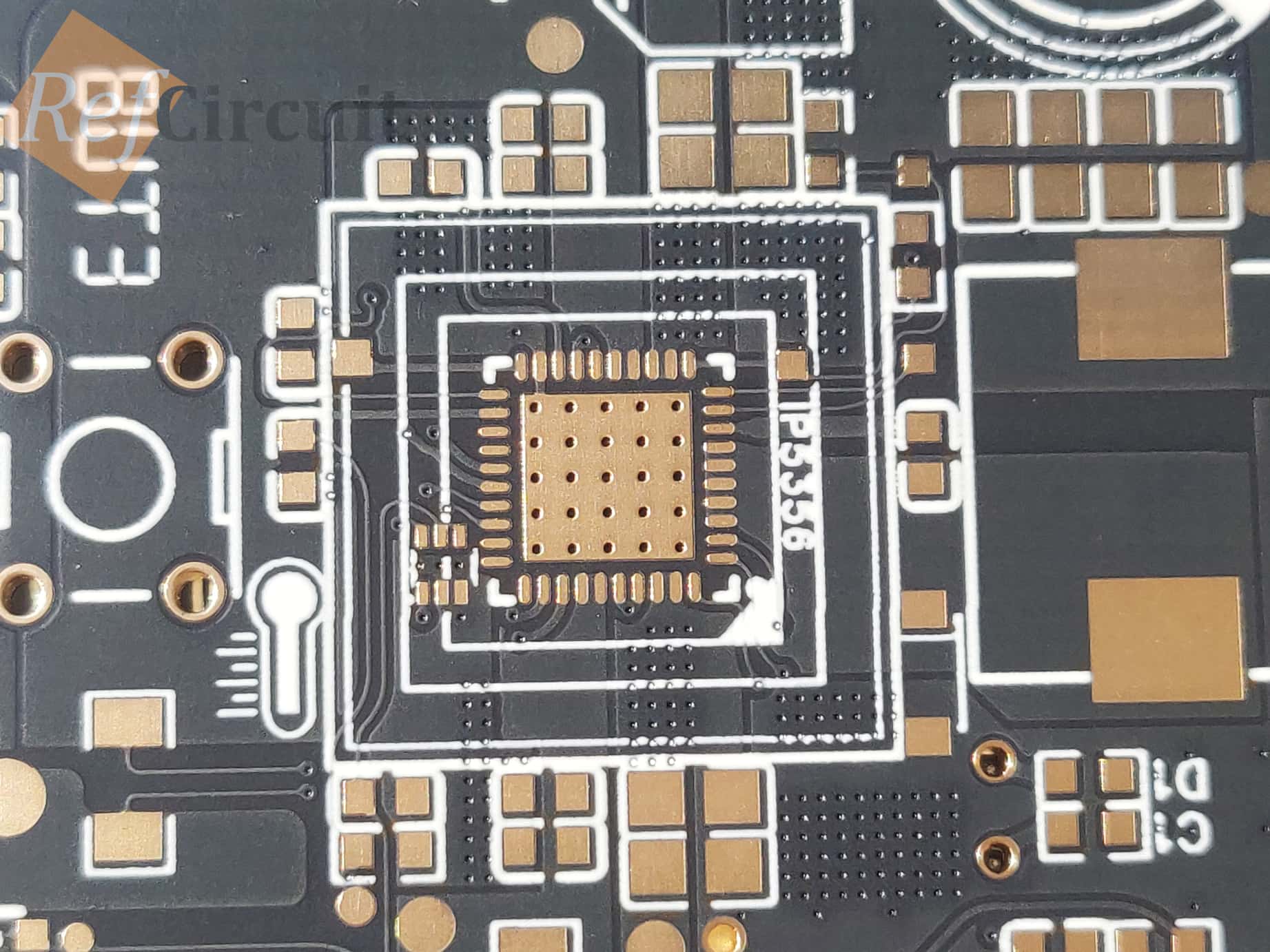 |  |
 |  |
 |  |
Conclusions
| 🟡 | For most boards edge plating not necessary at all, but it makes this board looks cooler |
| 🟢 | When design PCBs I recommend to make edge via stitching, it should be enough. Make offset 0.4mm (for V-cut) and place D0.45/d0.2mm or D0.6/d0.3mm vias across the perimeter. |